GM2501
GM2501 is P-CHANNEL ENHANCEMENT MODE POWER MOSFET manufactured by GTM.
Description
Features
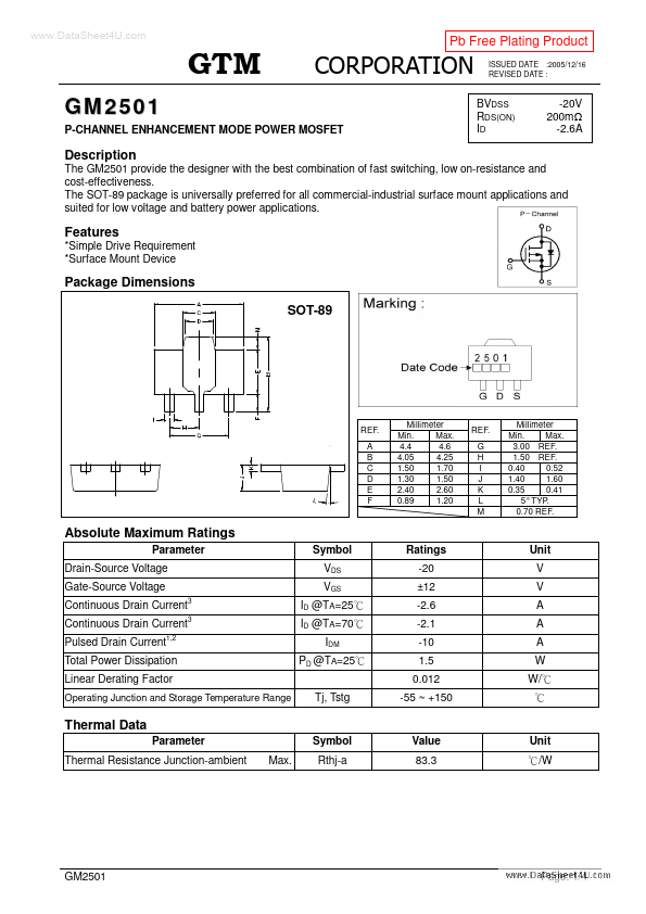
Package Dimensions SOT-89
REF. A B C D E F
Millimeter Min. Max. 4.4 4.6 4.05 4.25 1.50 1.70 1.30 1.50 2.40 2.60 0.89 1.20
REF. G H I J K L M
Millimeter Min. Max. 3.00 REF. 1.50 REF. 0.40 0.52 1.40 1.60 0.35 0.41 5° TYP. 0.70 REF.
Absolute Maximum Ratings
Parameter Drain-Source Voltage Gate-Source Voltage Continuous Drain Current Continuous Drain Current Pulsed Drain Current
1,2 3 3
Symbol VDS VGS ID @TA=25 ID @TA=70 IDM PD @TA=25 Tj, Tstg
Ratings -20 ±12 -2.6 -2.1 -10 1.5 0.012 -55 ~ +150
Unit V V A A A W W/
Total Power Dissipation Linear Derating Factor
Operating Junction and Storage Temperature Range
Thermal Data
Parameter Thermal Resistance Junction-ambient Max. Symbol Rthj-a Value 83.3 Unit /W
Page: 1/4
..
ISSUED DATE :2005/12/16 REVISED DATE :
Electrical Characteristics (Tj = 25
Parameter Drain-Source Breakdown Voltage
Breakdown Voltage Temperature Coefficient unless otherwise specified)
Min. -20 -0.5 Typ. -0.1 4.4 5.2 1.36 0.6 5.2 9.7 19 29 295 170 65 Max. ±100 -1 -10 200 250 300 10 p F ns n C m Unit V V/ V S n A u A u A Test Conditions VGS=0, ID=-250u A Reference to 25 , ID=-1m A VDS=VGS, ID=-250u A VDS=-5V, ID=-2.6A VGS= ±12V VDS=-20V, VGS=0 VDS=-16V, VGS=0 VGS=-10V, ID=-2.6A VGS=-4.5V, ID=-2.0A VGS=-2.5V, ID=-1.0A ID=-2.8A VDS=-6V VGS=-5V VDS=-15V ID=-1A VGS=-10V RG=6 RD=15 VGS=0V VDS=-6V f=1.0MHz
Symbol BVDSS
BVDSS / Tj
Gate Threshold Voltage Forward Transconductance Gate-Source Leakage Current
Drain-Source Leakage Current(Tj=25 ) Drain-Source Leakage Current(Tj=70 )
VGS(th) gfs IGSS IDSS
Static Drain-Source On-Resistance
RDS(ON)
- Total Gate Charge2 Gate-Source Charge Gate-Drain (“Miller”) Change Turn-on Delay Time2 Rise Time Turn-off Delay Time Fall Time Input Capacitance Output Capacitance Reverse Transfer Capacitance
Qg Qgs Qgd Td(on) Tr Td(off) Tf Ciss Coss Crss
- Source-Drain Diode
Parameter Forward On Voltage
Symbol VSD IS...