GP34119
GP34119 is LOW POWER AUDIO AMPLIFIER manufactured by GTM.
Description
LOW POWER AUDIO AMPLIFIER
The GP34119 is a low power audio amplifier integrated circuit intended (primarily) for telephone applications, such as in speakerphones. It provides differential speaker outputs to maximize output swing at low supply voltages (2.0V minimum). Coupling capacitors to the speaker are not required. Open loop gain is 80 d B, and the closed loop gain is set with two external resistors. A Chip Disable pin permits powering down and/or muting the input signal.
Features
Wide Operating Supply Voltage Range (2.0V to 16V), Allows Telephone Line Powered Applications Low Quiescent Supply Current (2.7m A Typ) for Battery Powered Applications Chip Disable Input to Power Down the IC Low Power-Down Quiescent Current (65u A Typ) Drives a Wide Range of Speaker Loads (8.0 Output Power Exceeds 250 m W with 32 Low Total Harmonic Distortion (0.5% Typ) Gain Adjustable from <0 d B to >46 d B for Voice Band Requires Few External ponents and Up) Speaker
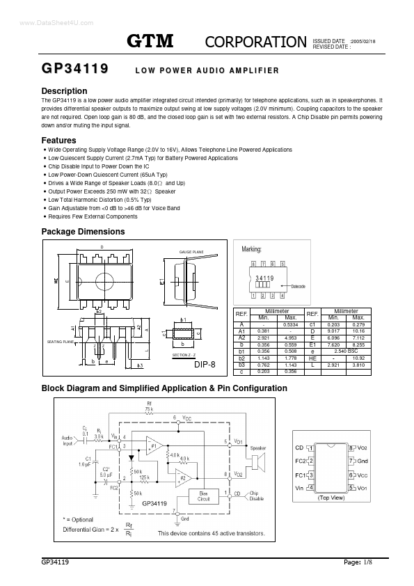
Package Dimensions
GAUGE PLANE
REF. A A1 A2 b b1 b2 b3 c
Millimeter Min. Max.
0.381 2.921 0.356 0.356 1.143 0.762 0.203 0.5334 4.953 0.559 0.508 1.778 1.143 0.356
REF. c1 D E E1 e HE L
Millimeter Min. Max.
0.203 0.279 9.017 10.16 6.096 7.112 7.620 8.255 2.540 BSC 10.92 2.921 3.810
SEATING PLANE Z Z b
SECTION Z
- Z b e
DIP-8
Block Diagram and Simplified Application & Pin Configuration c
1/8
ISSUED DATE :2005/02/18 REVISED DATE :
Maximum Ratings
Rating
Supply Voltage Maximum Output Current at VO1, VO2 Maximum Voltage @ Vin, FC1, FC2, CD Applied Output Voltage to VO1, VO2 when disabled Junction Temperature
Note: ESD data available upon request.
Value -1.0 to +18 ±250 -1.0, VCC+1.0 -1.0, VCC+1.0 -55, +140
Unit Vdc m A Vdc
Remended Operating Conditions
Characteristics Supply Voltage Voltage @ CD (Pin 1) Load Impedance Peak Load Current Differential Gain (5.0k Hz Bandwidth) Ambient Temperature
Symbol VCC VCD RL IL AVD TA
Min +2.0 0 8.0 0 -20 Test Conditions
Max +16 VCC ±200 46 +70 Min 80...