GS411SD
GS411SD is SURFACE MOUNT SCHOTTKY BARRIER DIODE manufactured by GTM.
..
CORPORATION
G S 4 11 S D
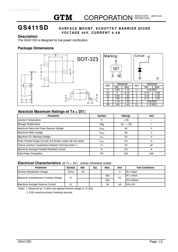
Description Package Dimensions
ISSUED DATE :2005/12/20 REVISED DATE :
S U R F A C E M O U N T, S C H O T T K Y B A R R I E R D I O D E V O LT A G E 4 0 V, C U R R E N T 0 . 5 A
The GS411SD is designed for low power rectification.
REF. A A1 A2 D E HE
Millimeter Min. Max. 0.80 1.10 0 0.10 0.80 1.00 1.80 2.20 1.15 1.35 1.80 2.40
REF. L1 L b c e Q1
Millimeter Min. Max. 0.42 REF. 0.15 0.35 0.25 0.40 0.10 0.25 0.65 REF. 0.15 BSC.
Absolute Maximum Ratings at TA = 25
Parameter Junction Temperature Storage Temperature Maximum Recurrent Peak Reverse Voltage Maximum RMS Voltage Maximum DC Blocking Voltage Peak Forward Surge Current at 8.3m Sec single half sine-wave Typical Junction Capacitance between Terminal (Note 1) Maximum Average Forward Rectified Current Total Power Dissipation Symbol Tj Tstg VRRM VRMS VDC IFSM CJ Io PD Ratings +125 -40 ~ +125 40 28 20 3.0 20 0.5 225 V V V A p F A m W Unit
Electrical Characteristics (at TA = 25
Parameter Reverse Breakdown Voltage Maximum Instantaneous Forward Voltage Maximum Average Reverse Current Symbol V(BR)R VF IR unless otherwise noted)
Min. 40 Typ. Max. 300 500 30 Unit V m V u A Test Conditions IR=100 A IF1=10m A IF2=500m A VR=10V
Notes: 1. Measured at 1.0 MHz and applied reverse voltage of 10 volts. 2. ESD sensitive product handling required.
Page: 1/2
CORPORATION
Characteristics Curve
ISSUED DATE :2005/12/20 REVISED DATE :
Important Notice: All rights are reserved. Reproduction in whole or in part is prohibited without the prior written approval of GTM. GTM reserves the right to make changes to its products without notice. GTM semiconductor products are not warranted to be suitable for use in life-support Applications, or systems. GTM assumes no liability for any consequence of customer product design, infringement of patents, or application assistance. Head Office And Factory: Taiwan: No. 17-1 Tatung Rd. Fu Kou Hsin-Chu Industrial Park, Hsin-Chu, Taiwan, R. O. C....