GSN202U
GSN202U is SWITCHING DIODE manufactured by GTM.
..
ISSUED DATE :2004/09/24 REVISED DATE :
Description
S U R F A C E M O U N T, S W I T C H I N G D I O D E V O LT A G E 8 0 V, C U R R E N T 0 . 1 A
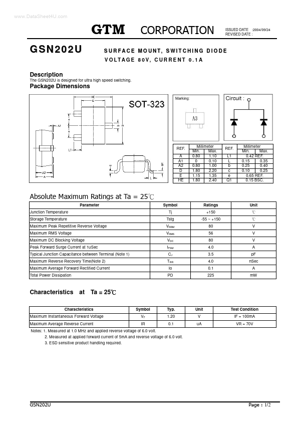
Package Dimensions
The GSN202U is designed for ultra high speed switching.
REF. A A1 A2 D E HE
Millimeter Min. Max. 0.80 1.10 0 0.10 0.80 1.00 1.80 2.20 1.15 1.35 1.80 2.40
REF. L1 L b c e Q1
Millimeter Min. Max. 0.42 REF. 0.15 0.35 0.25 0.40 0.10 0.25 0.65 REF. 0.15 BSC.
Parameter Junction Temperature Storage Temperature Maximum Peak Repetitive Reverse Voltage Maximum RMS Voltage Maximum DC Blocking Voltage Peak Forward Surge Current at 1u Sec Typical Junction Capacitance between Terminal (Note 1) Maximum Reverse Recovery Time(Note 2) Maximum Average Forward Rectified Current Total Power Dissipation
Symbol Tj Tstg VRRM VRMS VDC IFSM CJ TRR Io PD
Ratings +150 -55 ~ +150 80 56 80 4.0 3.5 4.0 0.1 225
Unit
V V V A p F n Sec A m W
Characteristics at Ta = 25
Symbol VF IR Typ. 1.20 0.1 Unit V u A Test Condition IF = 100m A VR = 70V
Characteristics Maximum Instantaneous Forward Voltage Maximum Average Reverse Current
Notes: 1. Measured at 1.0 MHz and applied reverse voltage of 6.0 volt. 2. Measured at applied forward current of 5m A and reverse voltage of 6.0 volt. 3. ESD sensitive product handling required.
1/2
ISSUED DATE :2004/09/24 REVISED DATE :
Characteristics Curve
Important Notice: All rights are reserved. Reproduction in whole or in part is prohibited without the prior written approval of GTM. GTM reserves the right to make changes to its products without notice. GTM semiconductor products are not warranted to be suitable for use in life-support Applications, or systems. GTM assumes no liability for any consequence of customer product design, infringement of patents, or application assistance. Head Office And Factory: Taiwan: No. 17-1 Tatung Rd. Fu Kou Hsin-Chu Industrial Park, Hsin-Chu, Taiwan, R. O. C. TEL : 886-3-597-7061 FAX : 886-3-597-9220, 597-0785 China: (201203)...