GSS4501
GSS4501 is POWER MOSFET manufactured by GTM.
..
Pb Free Plating Product
ISSUED DATE :2005/08/24 REVISED DATE :2006/11/09C
N AND P-CHANNEL ENHANCEMENT MODE POWER MOSFET
The GSS4501 provide the designer with the best bination of fast switching, ruggedized device design, low on-resistance and cost-effectiveness. The SOP-8 package is universally preferred for all mercial-industrial surface mount applications and suited for low voltage applications such as DC/DC converters.
- Simple Drive Requirement
- Lower On-resistance
- Fast Switching
Description
N-CH BVDSS 30V N-CH RDS(ON) 28m N-CH ID 7A P-CH BVDSS -30V N-CH RDS(ON) 50m N-CH ID -5.3A
Features
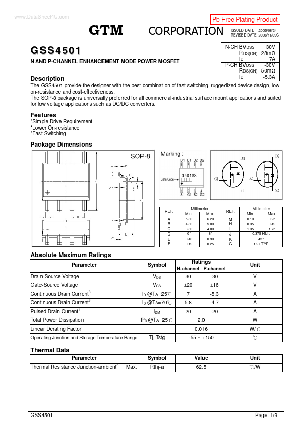
Package Dimensions
REF. A B C D E F
Millimeter Min. Max.
5.80 4.80 3.80 0° 0.40 0.19 6.20 5.00 4.00 8° 0.90 0.25
REF. M H L J K G
Millimeter Min. Max.
0.10 0.25 0.35 0.49 1.35 1.75 0.375 REF. 45° 1.27...