Datasheet4U Logo Datasheet4U.com

GFB75N03 - N-Channel Enhancement-Mode MOSFET

Datasheet Summary

Features

  • Advanced Trench Process Technology.
  • High Density Cell Design for Ultra Low On-Resistance.
  • Specially Designed for Low Voltage DC/DC Converters.
  • Fast Switching for High Efficiency Maximum Ratings and Thermal Characteristics (T Parameter Drain-Source Voltage Gate-Source Voltage Continuous Drain Current(1) Pulsed Drain Current Maximum Power Dissipation TA = 25°C TA = 100°C Symbol VDS VGS ID IDM PD TJ, Tstg TL RθJC (2) C = 25°C unless otherwise noted) Limit 30.

📥 Download Datasheet

Datasheet preview – GFB75N03

Datasheet Details

Part number GFB75N03
Manufacturer General Semiconductor
File Size 134.72 KB
Description N-Channel Enhancement-Mode MOSFET
Datasheet download datasheet GFB75N03 Datasheet
Additional preview pages of the GFB75N03 datasheet.
Other Datasheets by General Semiconductor

Full PDF Text Transcription

Click to expand full text
www.DataSheet4U.com GFB75N03 N-Channel Enhancement-Mode MOSFET H C N t E ET c u R d T ENF ro P G New ® VDS 30V RDS(ON) 6.5mΩ ID 80A
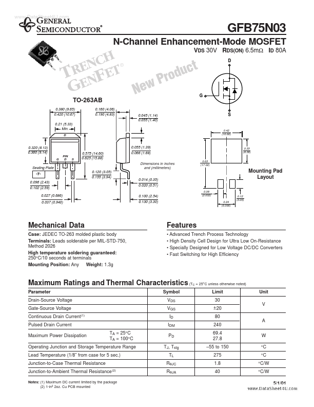
 D TO-263AB 0.380 (9.65) 0.420 (10.67) 0.21 (5.33) Min. D G 0.160 (4.06) 0.190 (4.83) 0.045 (1.14) 0.055 (1.40) S 0.42 (10.66) 0.320 (8.13) 0.360 (9.14) G PIN D S 0.575 (14.60) 0.625 (15.88) 0.055 (1.39) 0.066 (1.68) Dimensions in inches and (millimeters) 0.63 (17.02) 0.33 (8.38) Seating Plate -T0.096 (2.43) 0.102 (2.59) 0.027 (0.686) 0.037 (0.940) 0.120 (3.05) 0.155 (3.94) 0.014 (0.35) 0.020 (0.51) 0.100 (2.54) 0.130 (3.30) 0.08 (2.032) 0.24 (6.096) 0.12 (3.
Published: |