HCD310
HCD310 is OCXO Low Profile manufactured by Golledge Electronics.
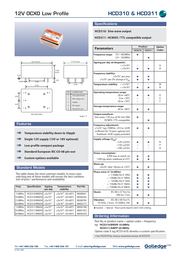
12V OCXO Low Profile
HCD310 & HCD311
Specifications
HCD310: Sine wave output HCD311: HCMOS / TTL patible output
Parameters
Frequency range:
36.10 (max) 27.20 (max)
Product
HCD310 HCD311
Option Codes
5.0 ~ 60.0MHz 5.0 ~ 50.0MHz
˿ ˿ ˿ ˿ M N D E F A B
15.00 (max) 0.50 0.80Ø 17.80 25.40 PIN 1 2 8.90 1 BOTTOM VIEW 5 2 3 4 5 5.00 15.00
Ageing per day (at despatch): < ±1x10⁻⁸ < ±5x10⁻⁹ Frequency stability: ±5x10⁻⁷ per year ±1x10⁻⁷ per 5% change in VDD Temperature stability: < ±1x10⁻⁷ < ±5x10⁻⁸
˿ ˿ ˿ ˿
3 8.90
CONNECTION Freq adjustment Ref. voltage out Supply RF output Ground & case
Operating temperature range: -20 to +60°C 0 to +70°C -20 to +70°C Storage temperature range: -40 to +90°C Output waveform: Sine wave, 1.5V p-p ±0.5V into 50⏲ HCMOS / TTL patible Frequency adjustment: ±1x10⁻⁵ typ (10MHz), +0.5 to +6.0V (sufficient for 10 years ageing min) Stabilised +6.0V supply provided Supply voltage (VDD): +12V (±0.5V) +15V (±0.5V) +18V (±0.5V) Power consumption: 4.5W max at switch on 1.0W typ when stabilised at 25°C Warm up: ±5x10⁻⁸ after 10mins at +25°C Phase noise (@ 10.0MHz): < -110d Bc/Hz @ 10Hz < -130d Bc/Hz @ 100Hz < -145d Bc/Hz @ 1k Hz < -150d Bc/Hz @ 10k Hz < -150d Bc/Hz @ 50k Hz Shock: IEC 68-2-27 Test Ea 50G for 11ms
Scale 1:1
Features
« « « « «
Temperature stability down to 50ppb Single 12V supply (15V or 18V optional) Low profile pact package Standard European IEC CO-08 pin-out Custom options available
˿ ˿
˿ ˿
Standard Models
The table shows the most mon models. In most cases selecting one of these models will ensure the best bination of price / performance and availability.
Freq 5.0MHz 10.0MHz 13.0MHz 50.0MHz 5.0MHz 10.0MHz 50.0MHz Specification HCD310/BNDN HCD310/BNDN HCD310/BNDN HCD310/BNDN HCD311/BNDN HCD311/BNDN HCD311/BNDN Ageing per day ±5x10⁻⁹ ±5x10⁻⁹ ±5x10⁻⁹ ±5x10⁻⁹ ±5x10⁻⁹ ±5x10⁻⁹ ±5x10⁻⁹ Temperature stability ±5x10⁻⁸ -20+60°C ±5x10⁻⁸...