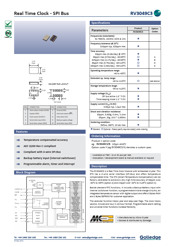
RV3049C3 Description
The RV3049C3 is a Real Time Clock Module with embedded crystal. This RTC has a 4-wire serial interface (SPI-Bus) and offers temperature pensated time. The STC (Smart Temperature pensation) can be factory calibrated to achieve a very high time accuracy of ±6ppm over -40°C to +85°C (option A) and ± 8ppm over -40°C to +125°C (option C).
RV3049C3 Key Features
- Option Codes
- Time accuracy: ±3ppm max (0.26s/day) @ 25°C
- Extended op. temp range: -40 to +125°C
- Supply voltage (VDD): SPI bus active 1.8 ~ 5.5V
- Standard. Optional
- Please specify required code(s) when ordering
- Available on T&R
- 1k or 3k pcs per reel
- Evaluation / development board & manual available on request
- Manufactured by Micro Crystal