Golledge MCSO2LW
the MCSO2LW please use the configurable options form to choose the options you require and then submit your configured product to our team.| Part No. | MCSO2LW |
|---|---|
| Datasheet | MCSO2LW Download |
| Manufacturer |  Golledge |
| Description | 2.5V LowJitter Oscillator |
| Buy | Stock & Price |
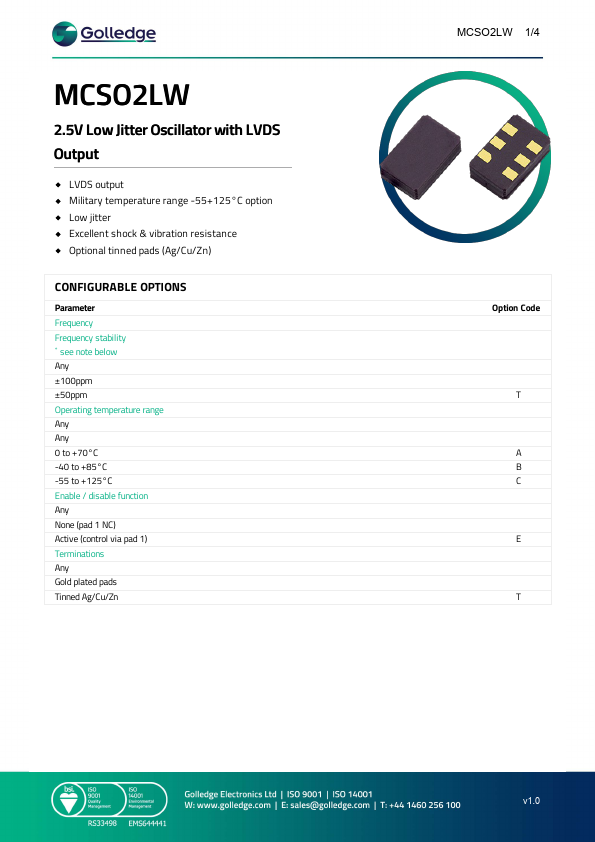
MCSO2LW 2.5V Low Jitter Oscillator with LVDS Output LVDS output Military temperature range -55+125°C option Low jitter Excellent shock & vibration resistance Optional tinned pads (Ag/Cu/Zn) CONFIGURABLE OPTIONS Parameter Frequency Frequency stability * see note below Any ±100ppm ±50ppm Operating temperature range Any Any 0 to +70°C -40 to +85°C -55 to +125°C Enable / disable function Any None (pad 1 NC) Active (control via pad 1) Terminations Any Gold plated pads Tinned Ag/Cu/Zn MCSO2LW 1/4 Option Code T A B C E T v1.0 MCSO2LW 2/4 SPECIFICATIONS Frequency range Dimensions Supply voltage (VDD) Storage temperature range Supply current Output Output load Logic levels (typ) Start up time Waveform symmetry Jitter RMS Rise / fall time Phase noise (typ @ 100MHz) Shock resistance Vibration resistance Soldering condition 40.0 ~ 130MHz 5.0 x 3.2 x 1.7mm +2.5V (±5%) -65 to +125°C 5mA max (@40.0MHz) 10mA max (@100MHz) 20mA max (@130MHz) LVDS 100Ω ‘0’ level = +1.1V ‘1’ level = +1.4V 5ms max 45:55 m...