Good-Ark Semiconductor BSS84AKW
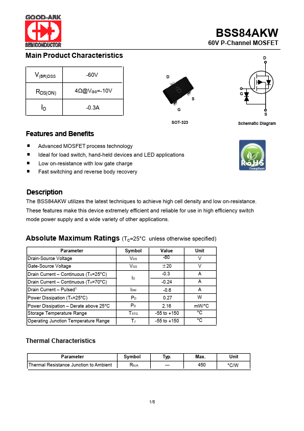
The BSS84AKW utilizes the latest techniques to achieve high cell density and low on-resistance. These features make this device extremely efficient and reliable for use in high efficiency switch mode power supply and a wide variety of other applications.| Part No. | BSS84AKW |
|---|---|
| Datasheet | BSS84AKW Download |
| Manufacturer |  Good-Ark Semiconductor |
| Description | 60V P-Channel MOSFET |
| Buy | Stock & Price |
FEATURES AND BENEFITS
Advanced MOSFET process technology Ideal for load switch, hand-held devices and LED applications Low on-resistance with low gate charge Fast switching and reverse body recovery G S Schematic DiagramDESCRIPTION
ABSOLUTE MAXIMUM RATINGS
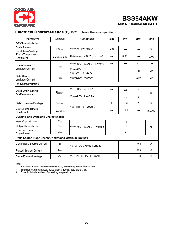
(TC=25°C unless otherwise specified) Parameter Drain-Source Voltage Gate-Source Voltage Drain Current – Continuous (TA=25°C) Drain Current – Continuous (TA=70°C) Drain Current – Pulsed1 Power Dissipation (TA=25°C) Power Dissipation – Derate above 25°C Storage Temperature Range Operating Junction Temperature Range Symbol VDS VGS ID IDM PD PD TSTG TJ Value -60 ±20 -0.3 -0.24 -0.6 0.27 2.16 -55 to +150 -55 to +150 Unit V V A A A W mW/°C °C °C Thermal Characteristics Parameter Symbol Typ. Thermal Resistance Junction to Ambient RθJA --- Max. 450 Unit °C/W 1/5 BSS84AKW 60V P-Channel MOSFETELECTRICAL CHARACTERISTICS
(TJ=25°C unless otherwise specified) Parameter Off Characteristics Drain-Source Breakdown Voltage BVDSS Temperature Coefficient Symbol Conditions Min.