Good-Ark Semiconductor BZX97
SILICON PLANAR ZENER DIODES
| Part No. | BZX97 |
|---|---|
| Datasheet | BZX97 Download |
| Manufacturer |  Good-Ark Semiconductor |
| Description | SILICON PLANAR ZENER DIODES |
| Buy | Stock & Price |
FEATURES
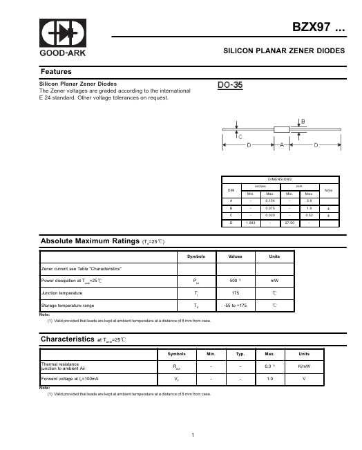
Silicon Planar Zener Diodes The Zener voltages are graded according to the international E 24 standard. Other voltage tolerances on request. DIM ENSIONS DIM A B C D inches Min. 1.083 Max. 0.154 0.075 0.020 Min. 27.50 mm Max. 3.9 1.9 0.52 NoteABSOLUTE MAXIMUM RATINGS
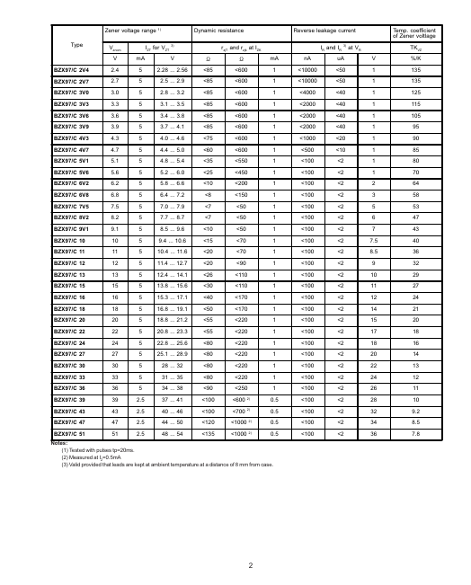
(Ta=25 ) Symbols Values Units Zener current see Table "Characteristics" Power dissipation at Tamb=25 Junction temperature Storage temperature range Ptot Tj TS 500 1) mW 175 -55 to +175 Note: (1) Valid provided that leads are kept at ambient temperature at a distance of 8 mm from case. Characteristics Thermal resistance junction to ambient Air at Tamb=25 Symbols Min. Typ. Max. Units RthA VF - - 0.3 1) K/mW V Forward voltage at IF=100mA 1.0 Note: (1) Valid provided that leads are kept at ambient temperature at a distance of 8 mm from case. 1 Zener voltage range Type Vznom V BZX97/C 2V4 BZX97/C 2V7 BZX97/C 3V0 BZX97/C 3V3 BZX97/C 3V6 BZX97/C 3V9 BZX97/C 4V3 BZX97/C 4V7 BZX97/C 5V1 BZX97/C 5V6 BZX97/C 6V2 BZX97/C 6V8...