Good-Ark Semiconductor GSBAT54SDW
Schottky Diode
| Part No. | GSBAT54SDW |
|---|---|
| Datasheet | GSBAT54SDW Download |
| Manufacturer |  Good-Ark Semiconductor |
| Description | Schottky Diode |
| Buy | Stock & Price |

FEATURES
● Low forward voltage drop● Fast switching
● PN junction guard ring for transient and ESD protection Schematic Diagram and Marking GSBAT54ADW GSBAT54BRW GSBAT54CDW GSBAT54xxW Series Schottky Diode GSBAT54SDW SOT-363 GSBAT54TW Marking: KL6 GSBAT54DW Marking: KLB GSBAT54JW Marking: KL7 Marking: KL8 Marking: KLA Marking: KLD Marking: KLC
ABSOLUTE MAXIMUM RATINGS
(TA=25°C unless otherwise noted) Parameter Symbol Value Repetitive Peak Reverse Voltage VRRM 30 Peak Working Reverse Voltage VRWM 30 DC Blocking Voltage VR 30 Forward Continuous Current IO 200 Repetitive Peak Forward Current IFRM 300 Non-repetitive Peak Forward Surge Current @t=8.3ms IFSM 600 Power Dissipation PD 200 Thermal Resistance From Junction To Ambient RΘJA 500 Junction Temperature TJ 125 Storage Temperature TSTG -55 to +150 Unit V V V mA mA mA mW °C/W °C °C 1/3 GSBAT54xxW Series Schottky DiodeELECTRICAL CHARACTERISTICS
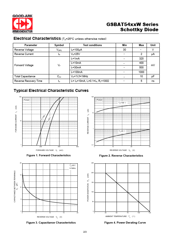
(TA=25°C unless otherwise noted) Parameter Reverse Voltage Reverse Current Forward Voltage To...