Good-Ark Semiconductor GSD107WS
Schottky Barrier Diode
| Part No. | GSD107WS |
|---|---|
| Datasheet | GSD107WS Download |
| Manufacturer |  Good-Ark Semiconductor |
| Description | Schottky Barrier Diode |
| Buy | Stock & Price |
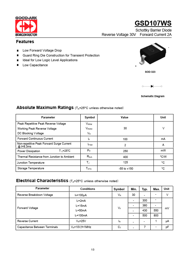
FEATURES
● Low Forward Voltage Drop● Guard Ring Die Construction for Transient Protection
● Ideal for Low Logic Level
APPLICATIONS
● Low Capacitance + SOD-323 Schematic DiagramABSOLUTE MAXIMUM RATINGS
(TA=25°C unless otherwise noted) Parameter Peak Repetitive Peak Reverse Voltage Working Peak Reverse Voltage DC Blocking V oltage Forward Continuous Current Non-repetitive Peak Forward Surge Current @ t=8.3ms Power Dissipation T C=25℃ Thermal Resistance from Junction to Ambient Junction Temperature Storage Temperature Symbol VRRM VRWM VR IF IFSM PD RθJA TJ TSTG Value 30 100 2 250 400 125 -55 to +150 Unit V mA A mW °C/W °C °CELECTRICAL CHARACTERISTICS
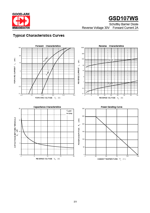
(TA=25°C unless otherwise noted) Parameter Reverse Breakdown Voltage Forward Voltage Reverse Current Capacitance Between Terminals Conditions IR=100µA IF=2mA IF=15mA IF=50mA IF=100mA VR=25V VR=10V,f=1MHz Symbol VR VF IR CT Min. 30 - - Typ. 300 360 430 500 7 Max. Unit -V mV 550 800 1 µA - pF 1/3 Typical Characteristics Curves GSD107WS Schot...