FEATURES AND BENEFITS
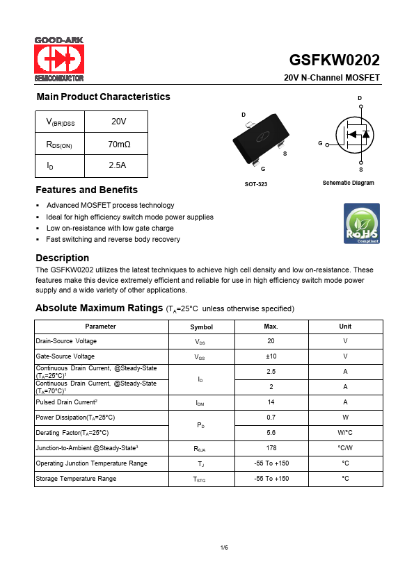
§ Advanced MOSFET process technology § Ideal for high efficiency switch mode power supplies § Low on-resistance with low gate charge § Fast switching and reverse body recovery S G SOT-323 G S Schematic Diagram DESCRIPTION
ABSOLUTE MAXIMUM RATINGS
(TA=25°C unless otherwise specified) Parameter Drain-Source Voltage Gate-Source Voltage Continuous Drain Current, @Steady-State (TA=25°C)1 Continuous Drain Current, @Steady-State (TA=70°C)1 Pulsed Drain Current2 Power Dissipation(TA=25°C) Derating Factor(TA=25°C) Junction-to-Ambient @Steady-State3 Operating Junction Temperature Range Storage Temperature Range Symbol VDS VGS ID IDM PD RθJA TJ TSTG Max. 20 ±10 2.5 2 14 0.7 5.6 178 -55 To +150 -55 To +150 Unit V V A A A W W/°C °C/W °C °C 1/6 GSFKW0202 20V N-Channel MOSFET ELECTRICAL CHARACTERISTICS
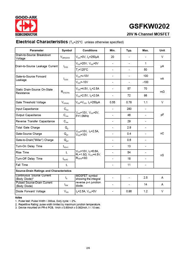
(TA=25°C unless otherwise specified) Parameter Drain-to-Source Breakdown Voltage Symbol V(BR)DSS Drain-to-Source Leakage Current IDSS Conditions VGS=0V, ID=250μA VDS=20V, VGS=0V T... Good-Ark Semiconductor