FEATURES AND BENEFITS
Advanced MOSFET process technology Ideal for battery operated systems, load switching, power converters and other general purpose applications Low on-resistance with low gate charge Fast switching and reverse body recovery DESCRIPTION
ABSOLUTE MAXIMUM RATINGS
(TA=25°C unless otherwise specified) Parameter Drain-Source Voltage Typical Gate-Source Voltage Continuous Drain Current1 Pulsed Drain Current (tp=10μs) Power Dissipation1 Thermal Resistance from Junction to Ambient1 Junction Temperature Storage Temperature Lead Temperature for Soldering Purposes(1/8” from case for 10 s) Symbol VDS VGS ID IDM PD RθJA TJ TSTG TL Value 20 ±12 0.75 1.8 150 833 150 -55 to +150 260 Unit V V A A mW °C /W °C °C °C 1/4 S3134K 20V N-Channel MOSFET ELECTRICAL CHARACTERISTICS
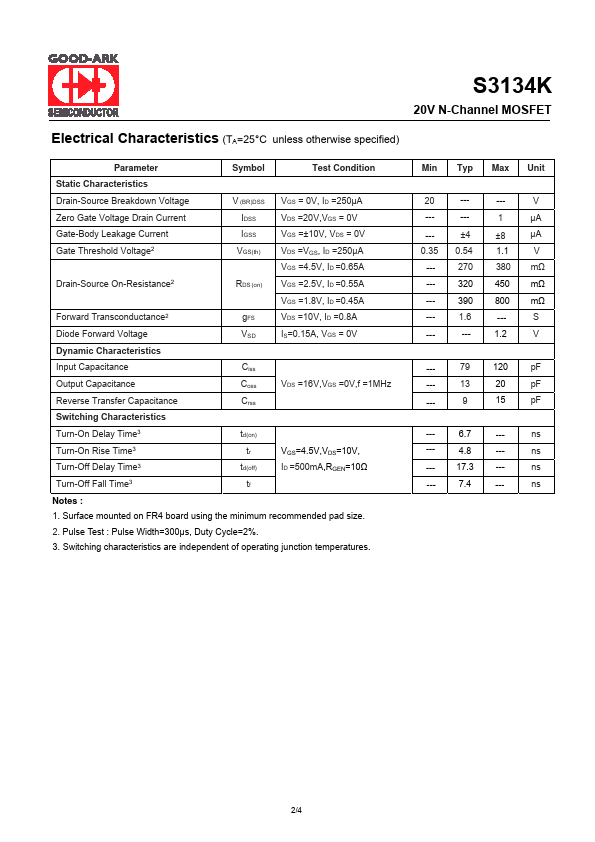
(TA=25°C unless otherwise specified) Parameter Symbol Test Condition Static Characteristics Drain-Source Breakdown Voltage V (BR)DSS VGS = 0V, ID =250µA Zero Gate Voltage Drain Current IDSS VDS =20V,VGS = 0... Good-Ark Semiconductor