Datasheet4U Logo Datasheet4U.com

HM10DP06D Datasheet P-channel Enhancement Mode Field Effect Transistor

Manufacturer: H&M Semiconductor

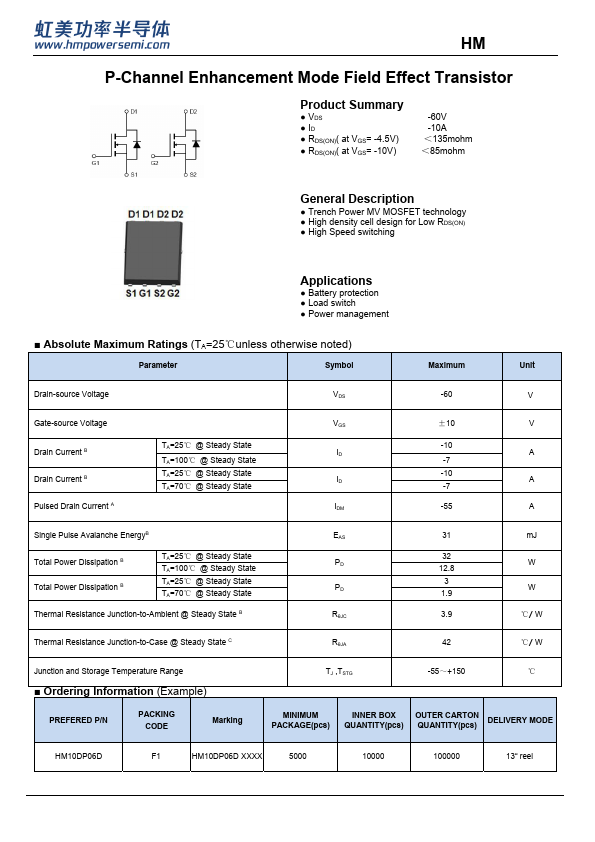
Overview: HM'3' P-Channel Enhancement Mode Field Effect Transistor  Product Summary ● VDS -60V ● ID -10A ● RDS(ON)( at VGS= -4.

General Description

● Trench Power MV MOSFET technology ● High density cell design for Low RDS(ON) ● High Speed switching Applications ● Battery protection ● Load switch ● Power management ■ Absolute Maximum Ratings (TA=25℃unless otherwise noted) Parameter Symbol Maximum Unit Drain-source Voltage VDS -60 V Gate-source Voltage VGS Drain Current B TA=25℃ @ Steady State TA=100℃ @ Steady State ID Drain Current B TA=25℃ @ Steady State TA=70℃ @ Steady State ID Pulsed Drain Current A IDM ±10 V -10 A -7 -10 -7 A -55 A Single Pulse Avalanche EnergyB EAS Total Power Dissipation B TA=25℃ @ Steady State TA=100℃ @ Steady State PD Total Power Dissipation B TA=25℃ @ Steady State TA=70℃ @ Steady State PD Thermal Resistance Junction-to-Ambient @ Steady State B RθJC 31 mJ 32 12.8 W 3 1.9 W 3.9 ℃/ W Thermal Resistance Junction-to-Case @ Steady State C RθJA 42 ℃/ W Junction and Storage Temperature Range ■ Ordering Information (Example) PREFERED P/N PACKING CODE Marking TJ ,TSTG -55~+150 ℃ MINIMUM PACKAGE(pcs) INNER BOX QUANTITY(pcs) OUTER CARTON QUANTITY(pcs) DELIVERY MODE HM10DP06D F1 HM10DP06D XXXX 5000 10000 100000 13“ reel ■ Electrical Characteristics (TJ=25℃ unless otherwise noted) Parameter Symbol Conditions Static Parameter  HM'3' Min Typ Max Units Zero Gate Voltage Drain Current IDSS VDS=-60V,VGS=0V,TC=25℃ -1 μA Gate-Body Leakage Current IGSS VGS= ±10V, VDS=0V ±100 nA Gate Threshold Voltage VGS(th) VDS= VGS, ID=-250μA -1.0 -3.0 V VGS= -4.5V, ID=-5A 135 Static Drain-Source On-Resistance Diode Forward Voltage RDS(ON) VSD VGS= -10V, ID=-1A IS=-60A,VGS=0V 85 mΩ -0.8 -1.2 V Maximum Body-Diode Continuous Current IS -10 A Dynamic Parameters Input Capacitance Ciss 2992 Output Capacitance Cos

HM10DP06D Distributor