HM18DP02Q Overview
Description
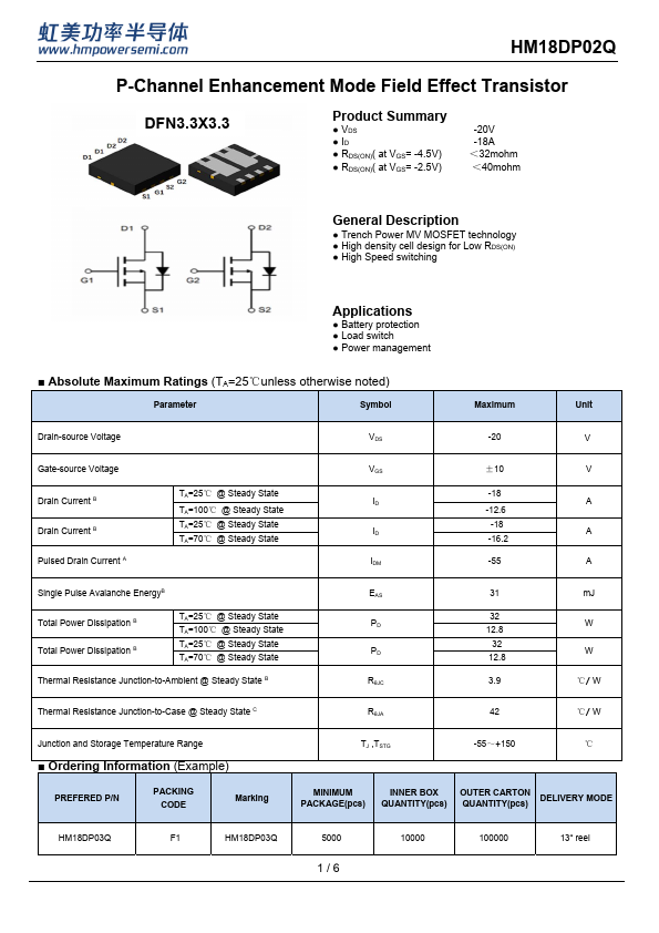
Trench Power MV MOSFET technology - High density cell design for Low RDS(ON) - High Speed switching.
| Part | HM18DP02Q |
|---|---|
| Description | P-Channel Enhancement Mode Field Effect Transistor |
| Category | Transistor |
| Manufacturer | H&M Semiconductor |
| Size | 908.97 KB |
Trench Power MV MOSFET technology - High density cell design for Low RDS(ON) - High Speed switching.
| Part Number | Manufacturer | Description |
|---|---|---|
| BDT88 | Inchange Semiconductor | Silicon PNP Power Transistor |
| KD333 | Tesla Elektronicke | Transistor |
| C828 | SEMTECH | NPN Silicon Transistor |