HM2310C
HM2310C is N-Channel Enhancement Mode Power MOSFET manufactured by H&M Semiconductor.
DESCRIPTION
The HM2310C is the N-Channel logic enhancement mode power field effect transistor is produced using high cell density, DMOS trench technology. This high-density process is especially tailored to minimize on-state resistance. These devices are particularly suited for low voltage application such as cellular phone and notebook puter power management and other battery powered circuits where high side switching.
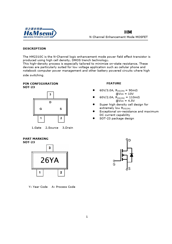
PIN CONFIGURATION SOT-23
FEATURE l- 60V/3.0A, RDS(ON) = 90mΩ @VGS = 10V l- 60V/2.0A, RDS(ON) = 110mΩ @VGS = 4.5V l- Super high density cell design for extremely low RDS(ON) l- Exceptional on-resistance and maximum DC current capability l- SOT-23 package design
1.Gate 2.Source 3.Drain
PART MARKING SOT-23
Y: Year Code A: Process Code 1
HM&
N Channel Enhancement Mode MOSFET
ABSOULTE MAXIMUM RATINGS (Ta = 25℃ Unless otherwise noted )
Parameter
Symbol Typical
Drain-Source Voltage
Gate-Source Voltage
Continuous Drain Current TJ=150℃)
TA=25℃ TA=70℃
Pulsed Drain Current
Continuous Source Current (Diode Conduction)
Power Dissipation
TA=25℃ TA=70℃
Operation Junction Temperature
VDSS VGSS
ID IDM IS PD TJ
±20 3.0 1.6 16
1.5 1.6 1.0 -55/150
Storgae Temperature Range
TSTG
-55/150
Thermal Resistance-Junction to Ambient
RθJA
Unit V V A A A W ℃ ℃ ℃/W
HM&
N Channel Enhancement Mode MOSFET
ELECTRICAL CHARACTERISTICS ( Ta = 25℃ Unless otherwise noted...