HM85N02K
Description
The HM85N02K uses advanced trench technology and design to provide excellent RDS(ON) with low gate charge. It can be used in a wide variety of applications.
General Features
- VDS =20V,ID =85A RDS(ON) <5.5mΩ @ VGS=4.5V
- High density cell design for ultra low Rdson
- Fully characterized avalanche voltage and current
- Good stability and uniformity with high EAS
- Excellent package for good heat dissipation
Application
- Load switching
- Hard switched and high frequency circuits
- Uninterruptible power supply
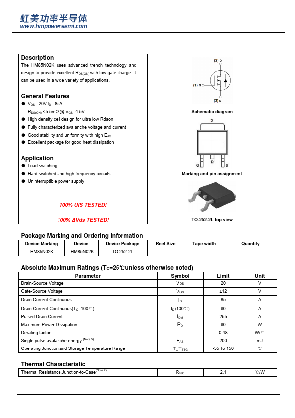
Schematic diagram 4
Marking and pin assignment
100% UIS TESTED!
100% ∆Vds TESTED!
TO-252-2L top view
Package Marking and Ordering Information
Device Marking
Device
Device Package
TO-252-2L
Reel Size
- Tape width
- Quantity
- Absolute Maximum Ratings (TC=25℃unless otherwise noted)
Parameter
Symbol
Drain-Source Voltage
Gate-Source Voltage
Drain Current-Continuous Drain Current-Continuous(TC=100℃)
ID (100℃)
Pulsed...