HD1H15A
Features
- VDSS=100V/VGSS=±20V/ID=15A RDS(ON)=105mΩ(Max.)@VGS=10V RDS(ON)=175mΩ(Max.)@VGS=4.5V
- ESD protect
- Reliable and Rugged
- High Density Cell Design For Ultra Low
On-Resistance
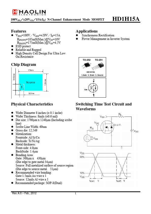
Chip Diagram
Applications
- Synchronous Rectification
- Power Management in Inverter System
TO-252 TO-251
HD1H15A 1.Gate 2. Drain 3. Source
Physical Characteristics
Switching Time Test Circuit and
Waveforms
- Wafer Diameter 8 inches (± 0.1 inche)
- Wafer Thickness: 8mils (±0.6 mil)
- Die size: 1700μm x 1240μm (Including scribe line)
- Scribe Line Width: 60um
- Gross die: 12,549
- Metalization:
Frontside: Al/Si/Cu Backside: Ti/Ni/Ag
- Metal thickness: Front-side: 4.0μm Back0side: 1.4μm
- Bonding Area: Gate: 300μm x 430μm (Die edge to gate metal 34μm) Source: Full metalized surface of source region (Die edge to source metal 51μm)
- Remended wire bonding: Gate:1.5mils Au wire x 1 Source: 12mils Al wire x 1
- Remended package: SOP-8(Dual)
Rev. A.0
- Feb., 2012
100VDS/±20VGS/15A(ID) N-Channel...