CD4081BD Overview
Key Specifications
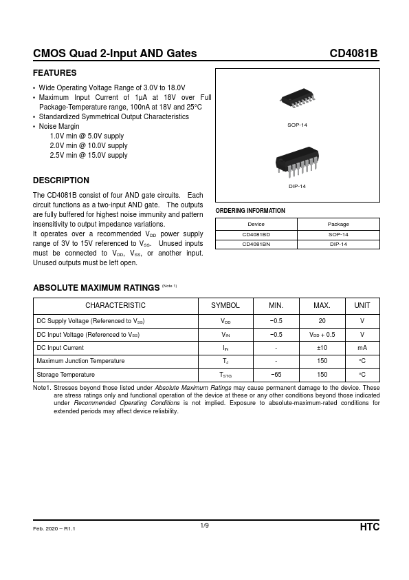
Package: DIP
Mount Type: Through Hole
Pins: 14
Operating Voltage: 5 V
Description
The CD4081B consist of four AND gate circuits. Each circuit functions as a two-input AND gate.
Key Features
- Wide Operating Voltage Range of 3.0V to 18.0V
- Maximum Input Current of 1µA at 18V over Full Package-Temperature range, 100nA at 18V and 25°C
- Standardized Symmetrical Output Characteristics
- Noise Margin 1.0V min @ 5.0V supply 2.0V min @ 10.0V supply 2.5V min @ 15.0V supply CD4081B SOP-14