FEATURES
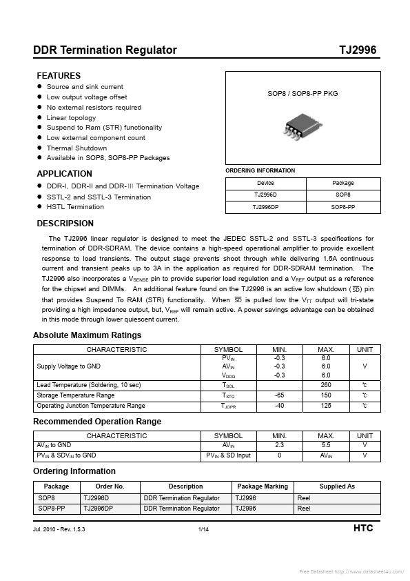
z z z z z z z z Source and sink current Low output voltage offset No external resistors required Linear topology Suspend to Ram (STR) functionality Low external component count Thermal Shutdown Available in SOP8, SOP8-PP Packages SOP8 / SOP8-PP PKG TJ2996 APPLICATION z DDR-I, DDR-II and DDR-Ⅲ Termination Voltage z SSTL-2 and SSTL-3 Termination z HSTL Termination ORDERING INFORMATION Device TJ2996D TJ2996DP Package SOP8 SOP8-PP DESCRIPSION The TJ2996 also incorporates a VSENSE pin to provide superior load regulation and a VREF output as a reference for the chipset and DIMMs. An additional feature found on the TJ2996 is an active low shutdown ( ) pin is pulled low the VTT output will tri-state that provides Suspend To RAM (STR) functionality. When providing a high impedance output, but, VREF will remain active. A power savings advantage can be obtained in this mode through lower quiescent current. ABSOLUTE MAXIMUM RATINGS
CHARACTERISTIC Supply Voltage to GND Lead Temperature (Soldering, 10 sec) Storage Temperature Range Operating Junction Temperature Range SYMBOL PVIN AVIN VDDQ TSOL TSTG TJOPR MIN. -0.3 -0.3 -0.3 -65 -40 MAX. HTC KOREA