TJ49300
TJ49300 is 3.0A Very Low Input / Output Voltage Ultra Low Dropout Linear Regulator manufactured by HTC KOREA.
FEATURES
Ultra Low Dropout Voltage Low Quiescent Current Excellent Line and Load Regulation Guaranteed Output Current of 3.0A Available in SOP-8-PP, TO-252, and TO-263 Packages Adjustable Output Voltage Down to 0.8V Fixed Output Voltages : 0.8V, 1.0V and 1.2V Logic Controlled Shutdown Option Over-Temperature/Over-Current Protection -40°C to 125°C Junction Temperature Range
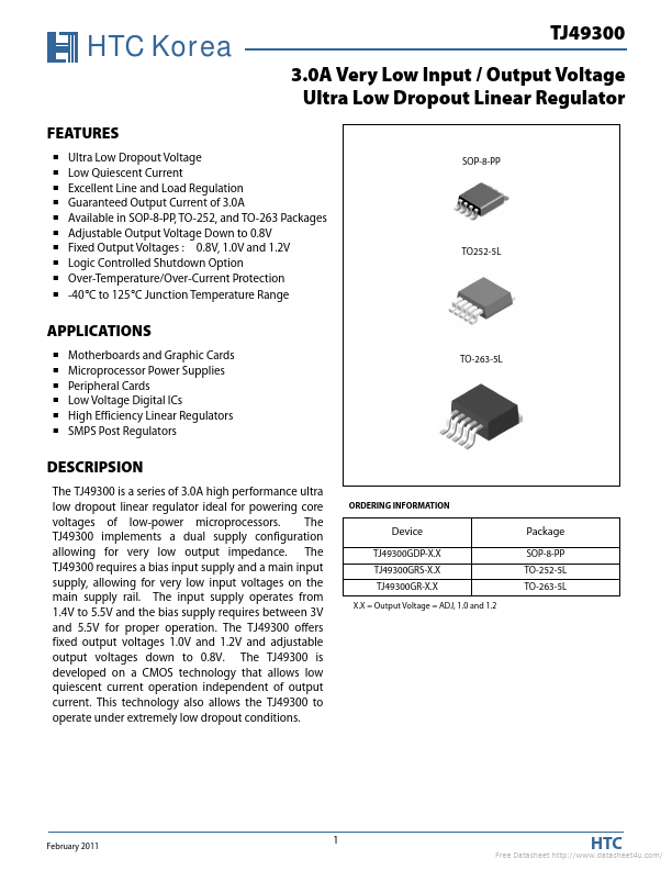
SOP-8-PP
TJ49300 3.0A Very Low Input / Output Voltage Ultra Low Dropout Linear Regulator
TO252-5L
APPLICATIONS
Motherboards and Graphic Cards Microprocessor Power Supplies Peripheral Cards Low Voltage Digital ICs High Efficiency Linear Regulators SMPS Post Regulators
TO-263-5L
DESCRIPSION
The TJ49300 is a series of 3.0A high performance ultra low dropout linear regulator ideal for powering core voltages of low-power microprocessors. The TJ49300 implements a dual supply configuration allowing for very low output impedance. The TJ49300 requires a bias input supply and a main input supply, allowing for very low input voltages on the main supply rail. The input supply operates from 1.4V to 5.5V and the bias supply requires between 3V and 5.5V for proper operation. The TJ49300 offers fixed output voltages 1.0V and 1.2V and adjustable output voltages down to 0.8V. The TJ49300 is developed on a CMOS technology that allows low quiescent current operation independent of output current. This technology also allows the TJ49300 to operate under extremely low dropout conditions.
ORDERING INFORMATION
Device
TJ49300GDP-X.X TJ49300GRS-X.X TJ49300GR-X.X
X.X = Output Voltage = ADJ, 1.0 and 1.2
Package
SOP-8-PP TO-252-5L TO-263-5L
February 2011
Free Datasheet http://../
ABSOLUTE MAXIMUM RATINGS
CHARACTERISTIC
Input Supply Voltage (Survival) Bias Supply Voltage (Survival) Enable Input Voltage (Survival) Output Voltage (Survival) Lead Temperature (Soldering, 5 sec) Storage Temperature Range
SYMBOL
VIN VBIAS VEN VOUT TSOL TSTG
MIN.
-0.3 -0.3 -0.3 -0.3
MAX.
6...