CSF501D
CSF501D is Silicon N-Channel Power MOSFET manufactured by HUAJING MICROELECTRONICS.
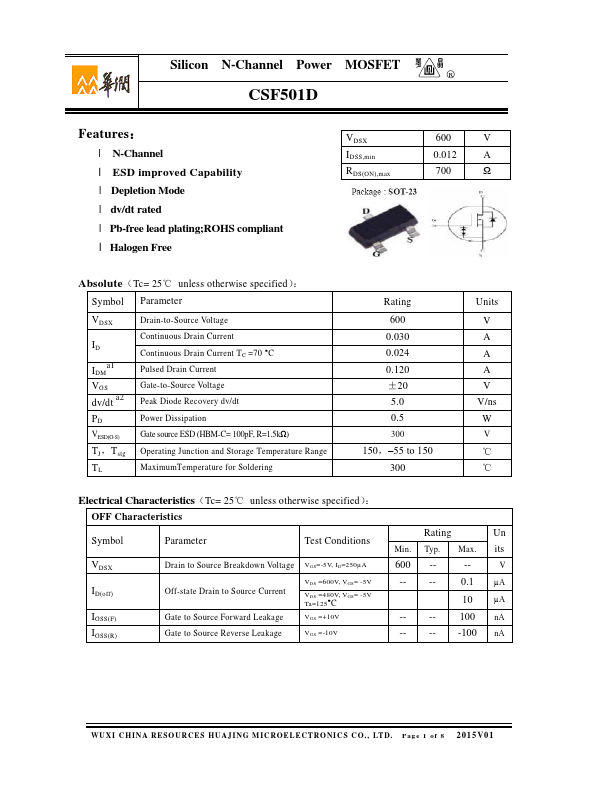
atures: l N-Channel l ESD improved Capability l Depletion Mode l dv/dt rated l Pb-free lead plating;ROHS pliant l Halogen Free
VDSX IDSS,min RDS(ON),max
600 0.012 700
V A Ω
Absolute(Tc= 25℃ unless otherwise specified):
Symbol Parameter
VDSX
ID a1
VGS dv/dt a2
VESD(G-S)
TJ,Tstg
Drain-to-Source Voltage Continuous Drain Current Continuous Drain Current TC =70 °C Pulsed Drain Current Gate-to-Source Voltage Peak Diode Recovery dv/dt Power Dissipation Gate source ESD (HBM-C= 100p F, R=1.5kΩ) Operating Junction and Storage Temperature Range Maximum Temperature for Soldering
Rating
600 0.030 0.024 0.120 ±20
5.0 0.5
150,- 55 to 150 300
Units
V A A A V V/ns W
℃ ℃
Electrical Characteristics(Tc= 25℃ unless otherwise specified):
OFF Characteristics
Symbol
Parameter
Test Conditions
VDSX
ID(off)
IGSS(F) IGSS(R)
Drain to Source Breakdown Voltage VGS=-5V, ID=250µA
Off-state Drain...