GENERAL DESCRIPTION
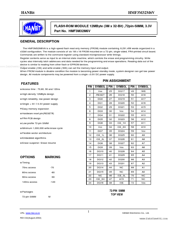
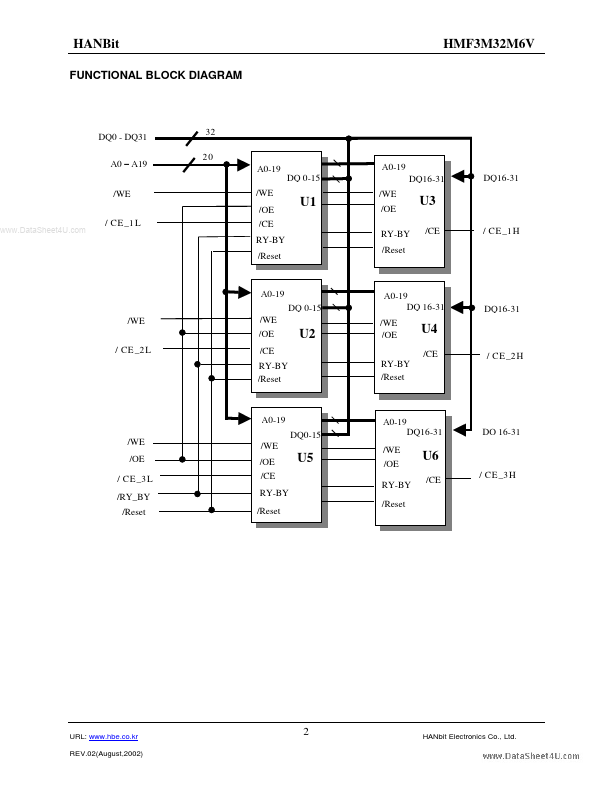
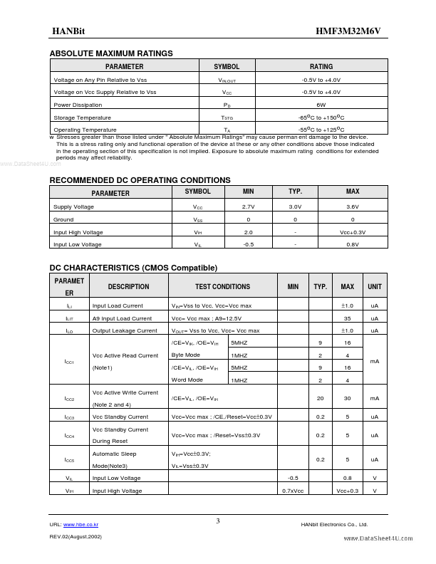
Commands are written to the command register using standard microprocessor write timings. Register contents serve as input to an internal state-machine, which controls the erase and programming circuitry. Write cycles also internally latch addresses and data needed for the programming and erase operations. Reading data out of the device is similar to reading from other flash or EPROM devices. Output enable (/OE) and write enable (/WE) can set the memory input and output. When FROM module is disable condition the module is becoming power standby mode, system designer can get low -power design. All module components may be powered from a single +3.0V DC power supply. FEATURES
w Access time : 70,80, 90 and 120ns w High-density 12MByte design w High-reliability, low-power design w Single + 3V ± 0.3V power supply w Easy memory expansion w Hardware reset pin(RESET#) w FR4-PCB design w Low profile 72-pin SIMM w Minimum 1,000,000 write/erase cycle w Flexible sector architec... Hanbit Electronics