GENERAL DESCRIPTION
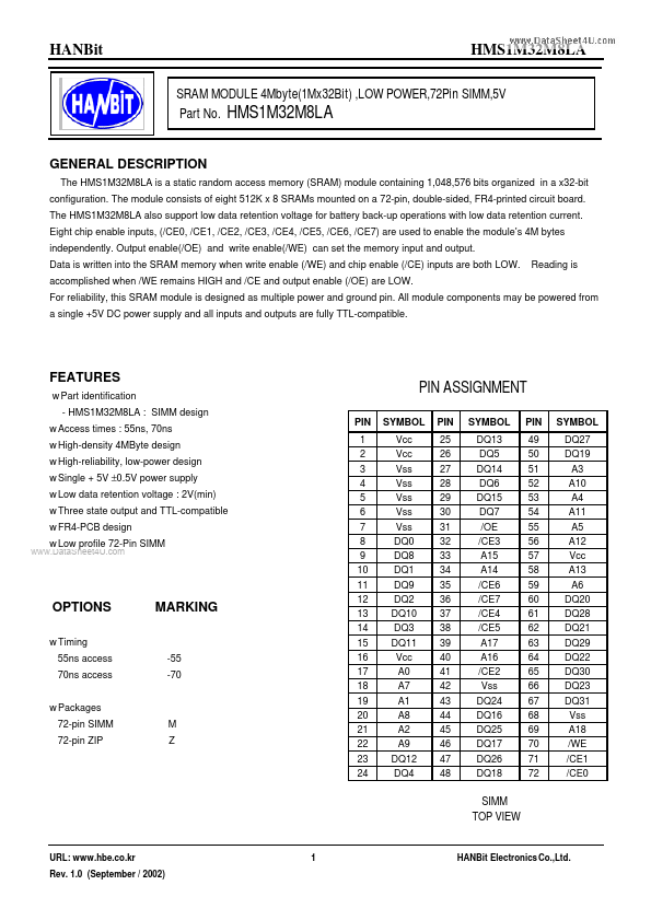
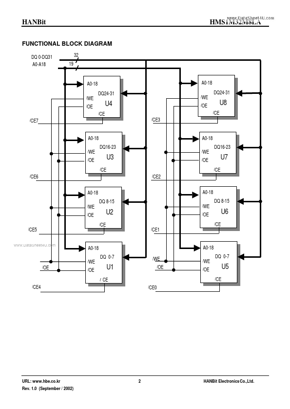
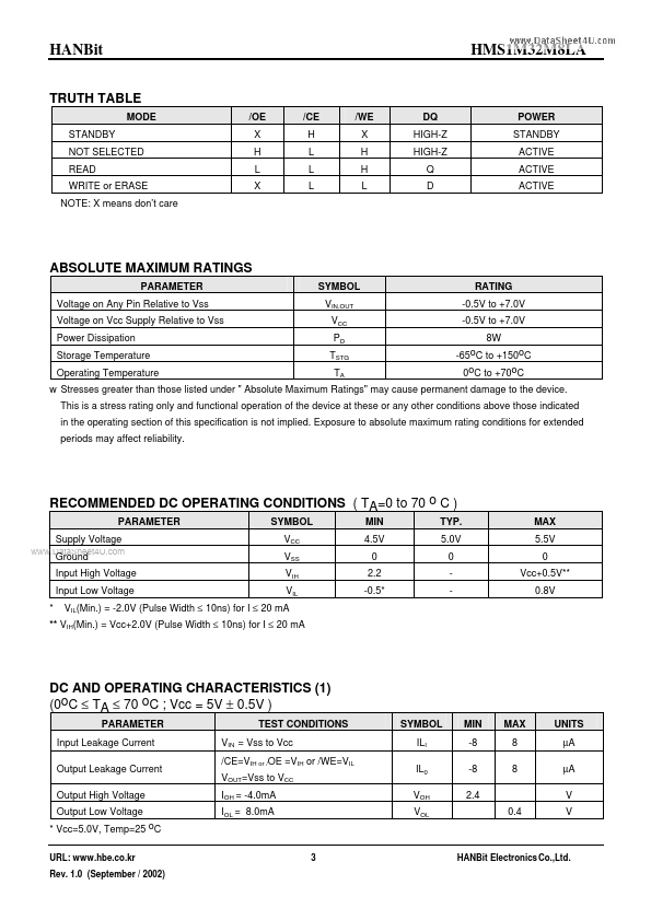
Eight chip enable inputs, (/CE0, /CE1, /CE2, /CE3, /CE4, /CE5, /CE6, /CE7) are used to enable the module’s 4M bytes independently. Output enable(/OE) and write enable(/WE) can set the memory input and output. Data is written into the SRAM memory when write enable (/WE) and chip enable (/CE) inputs are both LOW. accomplished when /WE remains HIGH and /CE and output enable (/OE) are LOW. For reliability, this SRAM module is designed as multiple power and ground pin. All module components may be powered from a single +5V DC power supply and all inputs and outputs are fully TTL-compatible. Reading is FEATURES
w Part identification - HMS1M32M8LA : SIMM design w Access times : 55ns, 70ns w High-density 4MByte design w High-reliability, low-power design w Single + 5V ±0.5V power supply w Low data retention voltage : 2V(min) w Three state output and TTL-compatible w FR4-PCB design PIN ASSIGNMENT PIN 1 2 3 4 5 6 7 8 9 10 11 12 13 14 15 16 17 18 19 20 21 22 23 24 SYMBOL Vcc V... Hanbit Electronics