2SD1420
Silicon NPN Epitaxial
Application
Low frequency power amplifier
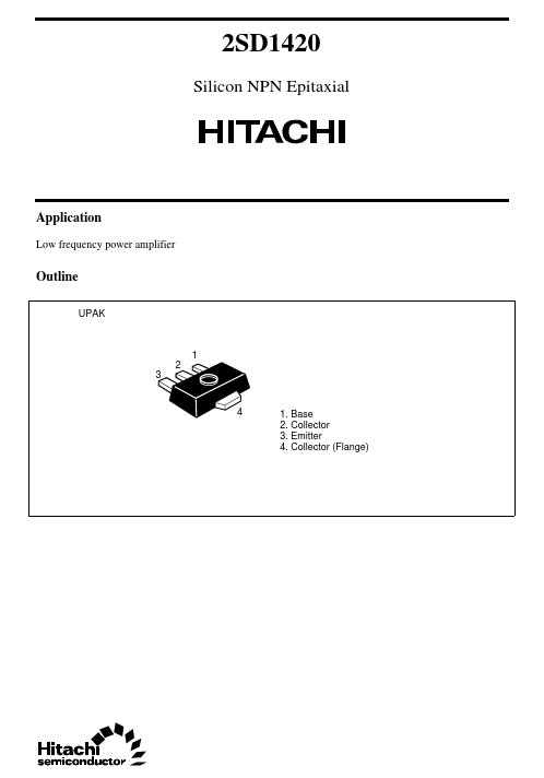
Outline
UPAK
1 3 2
1. Base 2. Collector 3. Emitter 4. Collector (Flange)
Absolute Maximum Ratings (Ta = 25°C)
Item Collector to base voltage Collector to emitter voltage Emitter to base voltage Collector current Collector peak current Collector power dissipation Junction temperature Storage temperature Symbol VCBO VCEO VEBO IC i C(peak)- PC
- Tj Tstg
2 1
Ratings 180 120 5 1.5 3 1 150
- 55 to +150
Unit V V V A A W °C °C
Notes: 1. PW ≤ 10 ms, Duty cycle ≤ 20% 2. Value on the alumina ceramic board (12.5 x 20 x 0.7 mm)
Electrical Characteristics (Ta = 25°C)
Item Collector to base breakdown voltage Symbol V(BR)CBO Min 180 120 5
- 1
Typ
- -
- -
- -
- -
Max
- -
- 10 320
- 1.0 0.9
Unit V V V µA
Test conditions I C = 1 m A, IE = 0 I C = 10 m A, RBE = ∞ I E = 1 m A, IC = 0 VCB = 160 V, IE = 0 VCE = 5 V, IC = 0.15 A VCE = 5 V, IC = 0.5 A
Collector to emitter breakdown V(BR)CEO voltage Emitter to base...