HD74AC14
Description
The HD74AC14 contains six logic inverters which accept standard CMOS input signals (TTL levels for HD74ACT14) and provide standard CMOS output levels. They are capable of transforming slowly changing input signals into sharply defined, jitter-free output signals. In addition, they have a greater noise margin than conventional inverters. The HD74AC14 has hysteresis between the positive-going and negative-going input thresholds (typically 1.0 V) which is determined internally by transistor ratios and is essentially insensitive to temperature and supply voltage variations.
Feature
- Outputs Source/Sink 24 m A
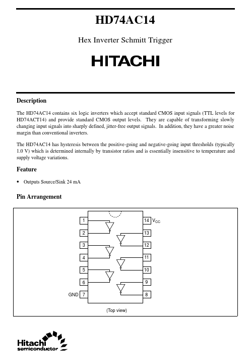
Pin Arrangement
1 2 3 4 5 6 GND 7 (Top view)
14 VCC 13 12 11 10 9 8
Function Table
Input A L H Output O H L
DC Characteristics (unless otherwise specified)
Item Maximum quiescent supply current Maximum quiescent supply current Maximum positive threshold Symbol I CC VCC (V) HD74AC14 40 HD74ACT14 Unit 40 µA Condition VIN = VCC or ground, VCC = 5.5 V, Ta =...