HD74HC563
Description
When the latch enable (LE) input is high, the Q outputs of HD74HC563 will follow the inversion of the D inputs and the Q outputs of HD74HC573 will follow the D inputs. When the latch enable goes low, data at the D inputs will be retained at the outputs until latch enable returns high again. When a high logic level is applied to the output control input, all outputs go to a high impedance state, regardless of what signals are present at the other inputs and the state of the storage elements.
Features
- -
- -
- High Speed Operation: tpd (Data to Q, Q) = 11 ns typ (CL = 50 p F) High Output Current: Fanout of 15 LSTTL Loads Wide Operating Voltage: VCC = 2 to 6 V Low Input Current: 1 µA max Low Quiescent Supply Current: ICC (static) = 4 µA max (Ta = 25°C)
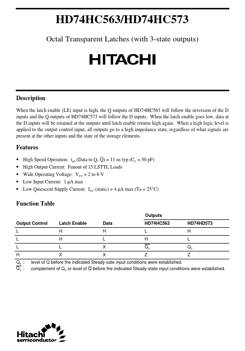
Function Table
Outputs Output Control L L L H Q0 : Q0 : Latch Enable H H L X Data H L X X HD74HC563 L H Q0 Z HD74HD573 H L Q0 Z level of Q before the indicated Steady-sate input conditions were established. plement of Q 0 or...