HD74HC597
Overview
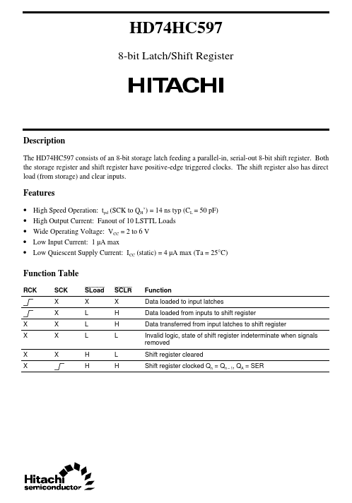
The HD74HC597 consists of an 8-bit storage latch feeding a parallel-in, serial-out 8-bit shift register. Both the storage register and shift register have positive-edge triggered clocks.
- High Speed Operation: tpd (SCK to QH’) = 14 ns typ (CL = 50 pF) High Output Current: Fanout of 10 LSTTL Loads Wide Operating Voltage: VCC = 2 to 6 V Low Input Current: 1 µA max Low Quiescent Supply Current: ICC (static) = 4 µA max (Ta = 25°C)