HN27C4000G Key Features
- Organization: 524288-word × 8-bit/262144word × 16-bit (BYTE /VPP enables selection byte-wide or word-wide)
- High speed: Access time 100 ns/120 ns/150 ns (max) Burst access time 50 ns/60 ns/60 ns (max)
- Low power dissipation: Standby mode; 5 µW (typ), Active mode; 150 mW/MHz (typ)
- Fast high reliability page programming, fast high-reliability programming and option programming: Program voltage; +12.5
- Inputs and outputs TTL patible during both read and program modes
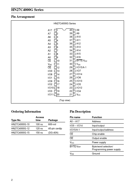
- Pin arrangement: 40-pin EIAJ standard pin patible with HN62414/ HN62434
- Device identifier mode: Manufacturer code and device code
- A17 I/O0
- I/O14 I/O15/A-1 CE OE VCC BYTE/VPP VSS Function Address Input/output Input/output/address Chip enable Output enable Powe
- I/O7, I/O8