Datasheet4U.com
🌙
K1762 Datasheet | Hitachi Semiconductor
Part:
K1762
Description:
2SK1762
Manufacturer:
Hitachi Semiconductor
Size:
62.64 KB
Download K1762 Datasheet PDF
Hitachi Semiconductor
K1762
Key Features
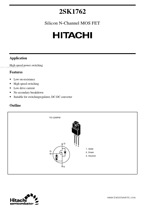
Low on-resistance High speed switching Low drive current No secondary breakdown Suitable for switchingregulator, DC-DC converter
×
Close