PF0342A
PF0342A is MOS FET Power Amplifier Module manufactured by Hitachi Semiconductor.
- Part of the PF0341A comparator family.
- Part of the PF0341A comparator family.
Features
- Small package: 30 × 10 × 5.9 mm
- High output power at low voltage: 2 W Typ at 4.8 V
- Low power control current: 200 µA Typ
Ordering Information
Type Name PF0341A PF0342A PF0343A PF0344A PF0345A Operating frequency 400 to 430 MHz 440 to 470 MHz 470 to 490 MHz 490 to 512 MHz 380 to 400 MHz
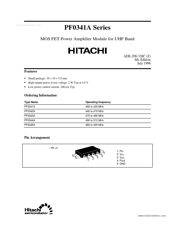
Pin Arrangement
- RF-J1 5 1 2 3 4 1: Pin 2: VPC 3: VDD 4: Pout 5: GND
..
PF0341A Series
Internal Diagram and External Circuit
G GND Pin1 Pin Pin2 VPC Pin3 VDD Pin4 Pout
G GND
Z1
C1
FB1
C3
C4
FB2
C2
Z2
Pin
Pout
C1 = C2 = 0.01 µF (Ceramic chip capacitor) C3 = C4 = 10 µF (Aluminum Electrolyte Capacitor) FB = Ferrite bead BL01RN1-A62-001 (Manufacture: MURATA) or equivalent Z1 = Z2 = 50 Ω (Microstrip line)
Absolute Maximum Ratings (Tc = 25°C)
Item Supply voltage Supply current PC voltage Input power Operating case temperature Storage temperature Symbol VDD I DD VPC Pin Tc (op) Tstg Rating 17 3 4.5 50
- 30 to +100
- 40 to +110 Unit V A V m W °C °C
..
PF0341A Series
Electrical Characteristics (Tc = 25°C)
Item Drain cutoff current Total efficiency 2nd harmonic distortion 3rd harmonic distortion Input VSWR Output power (1) Output power (2) Load VSWR tolerance Symbol I DS ηT 2nd H.D. 3rd H.D. VSWR (in) Pout (1) Pout (2)
- Min
- 35
- -
- 7 1.8 Typ
-...