ABSOLUTE MAXIMUM RATINGS
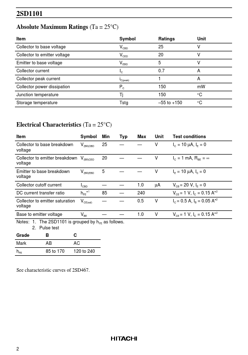
(Ta = 25°C) Item Collector to base voltage Collector to emitter voltage Emitter to base voltage Collector current Collector peak current Collector power dissipation Junction temperature Storage temperature Symbol VCBO VCEO VEBO IC iC(peak) PC Tj Tstg Ratings 25 20 5 0.7 1 150 150 –55 to +150 Unit V V V A A mW °C °C ELECTRICAL CHARACTERISTICS
(Ta = 25°C) Item Collector to base breakdown voltage Symbol V(BR)CBO Min 25 20 5 — 1 Typ — — — — — — — Max — — — 1.0 240 0.5 1.0 Unit V V V µA Test conditions I C = 10 µA, IE = 0 I C = 1 mA, RBE = ∞ I E = 10 µA, IC = 0 VCB = 20 V, IE = 0 VCE = 1 V, IC = 0.15 A*2 I C = 0.5 A, IB = 0.05 A*2 VCE = 1 V, IC = 0.15 A*2 Collector to emitter breakdown V(BR)CEO voltage Emitter to base breakdown voltage Collector cutoff current DC current transfer ratio Collector to emitter saturation voltage Base to emitter voltage V(BR)EBO I CBO hFE* 85 — — VCE(sat) VBE V V Notes: 1. The 2SD1101 is grouped by h FE as follows. 2. Pulse test Grade Mark hFE B AB 85 to 170 C AC 120 to 240 See characteristic curves of 2SD467. Hitachi