Hitachi 2SJ361
P-Channel MOSFET
| Part No. | 2SJ361 |
|---|---|
| Datasheet | 2SJ361 Download |
| Manufacturer |  Hitachi |
| Description | P-Channel MOSFET |
| Buy | Stock & Price |

FEATURES
●●
●
● Low on-resistance High speed switching Low drive current 2.5 V gate drive device can be driven from 3 V source Outline UPAK 2 1 4 D 1. Gate 2. Drain 3. Source 4. Drain S 3 G 2SJ361
ABSOLUTE MAXIMUM RATINGS
(Ta = 25°C) Item Drain to source voltage Gate to source voltage Drain current Drain peak current Body to drain diode reverse drain current Channel dissipation Channel temperature Storage temperature Symbol VDSS VGSS ID I D(pulse)* I DR Pch* Tch Tstg 2 1 Ratings –20 ±20 –2 –4 –2 1 150 –55 to +150 Unit V V A A A W °C °C Notes: 1. PW ≤ 10 µs, duty cycle ≤ 1% 2. Value on the alumina ceramic board (12.5×20×0.7 mm) 3. Marking is “RY”. 2 2SJ361ELECTRICAL CHARACTERISTICS
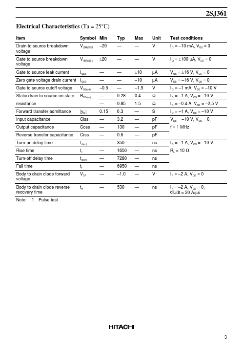
(Ta = 25°C) Item Drain to source breakdown voltage Gate to source breakdown voltage Gate to source leak current Symbol Min V(BR)DSS V(BR)GSS I GSS –20 ±20 — — –0.5 — — |yfs| Ciss Coss Crss t d(on) tr t d(off) tf VDF t rr 0.15 — — — — — — — — — Typ — — — — — 0.28 0.85 0.3 3.2 130 0.6 350 1650 7280 6950 –1.0...