ABSOLUTE MAXIMUM RATINGS
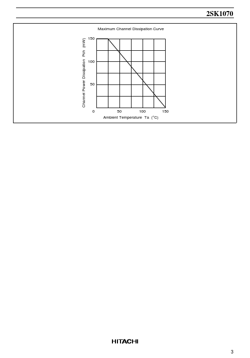
(Ta = 25°C) Item Gate to drain voltage Gate to source voltage Drain current Gate current Channel power dissipation Channel temperature Storage temperature Symbol VGDO VGSO ID IG Pch Tch Tstg Ratings –22 –22 50 10 150 150 –55 to +150 Unit V V mA mA mW °C °C ELECTRICAL CHARACTERISTICS
(Ta = 25°C) Item Gate cutoff current Gate to source breakdown voltage Drain current Gate to source cutoff voltage Forward transfer admittance Input capacitance Note: Grade Mark I DSS B PIB 6 to 14 C PIC 12 to 22 Symbol I GSS V(BR)GSS I DSS*1 VGS(off) y fs Ciss Min — –22 6 0 20 — D PID 18 to 30 Typ — — — — 30 9 E PIE 27 to 40 Max –10 — 40 –2.5 — — Unit nA V mA V mS pF Test conditions VGS = –15 V, VDS = 0 I G = –10 µA, VDS = 0 VDS = 5 V, VGS = 0, Pulse test VDS = 5 V, ID = 10 µA VDS = 5 V, VGS = 0, f = 1 kHz VDS = 5 V, VGS = 0, f = 1 MHz 1. The 2SK1070 is grouped by I DSS as follows. See characteristic curves of 2SK435. 2 2SK1070 Maximum Channel Dissipation Curve Channel Power Dissipa... Hitachi