Hitachi HA12220
The IC’s internal switches can be operated by sending control data from the HD49250. The signal timing is shown in figure 1, and the control commands are listed in table 1 and 2.| Part No. | HA12220 |
|---|---|
| Datasheet | HA12220 Download |
| Manufacturer |  Hitachi |
| Description | CD-ROM Drive Head Amplifier |
| Buy | Stock & Price |
FEATURES
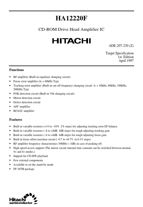
● Built-in variable resistors (+14 to –16% 2% steps) for adjusting tracking error EF balance● Built-in variable resistors (–8 to +8dB 4dB steps) for rough adjusting tracking gain
● Built-in variable resistors (–8 to +8dB 4dB steps) for rough adjusting focus gain
● Built-in focus offset insertion circuit (–0.7 to +0.7V in 0.1V steps)
● RF amplifier frequency characteristics 30MHz (–3dB) in case of peaking off
● High-speed access support (The mirror circuit internal time constant can be switched between normal, 4× and 8× modes.)
● Support for CD-RW playback
● Few external components
● Available to set the stand-by mode
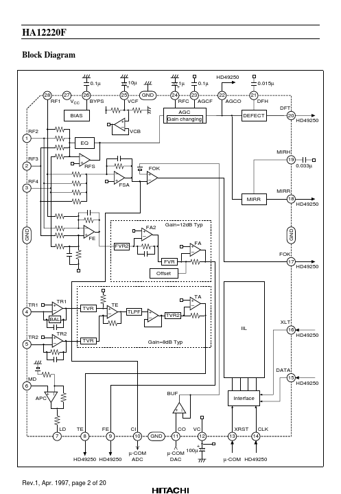
● FP-28TB package HA12220F Block Diagram 0.1µ 28 RF1 27 VCC BIAS RF2 1 + – EQ – + MIRH 19 RFS – + FSA FOK + – MIRR 18 HD49250 VCB 26 BYPS 10µ GND VCF 1µ 23 RFC AGCF 0.1µ HD49250 22 AGCO 21 DFH DEFECT DFT 20 HD49250 0.015µ 25 24 AGC Gain changing RF3 2 RF4 3 GND FE FVR2 + – FVR Offset FA FOK 17 HD49250 TR1 4 + – TR1 TVR + – TE TLPF + – TVR2 + – TA BAL TR2 5 + – TR...