Hitachi HD74AC107
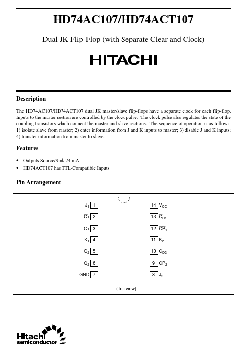
The HD74AC107/HD74ACT107 dual JK master/slave flip-flops have a separate clock for each flip-flop. The clock pulse also regulates the state of the coupling transistors which connect the master and slave sections. The sequence of operation is as follows: 1) isolate slave from master; 2) enter information from J and K inputs to master; 3) disable J and K inputs; 4) transfer information from master to slave.| Part No. | HD74AC107 |
|---|---|
| Datasheet | HD74AC107 Download |
| Manufacturer |  Hitachi |
| Description | Dual JK Flip-Flop (with Separate Clear and Clock) |
| Buy | Stock & Price |
DESCRIPTION
Inputs to the master section are controlled by the clock pulse.FEATURES
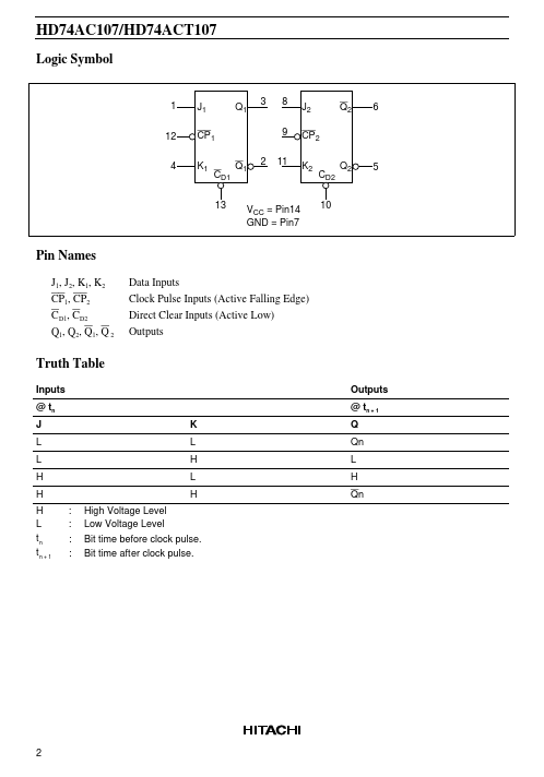
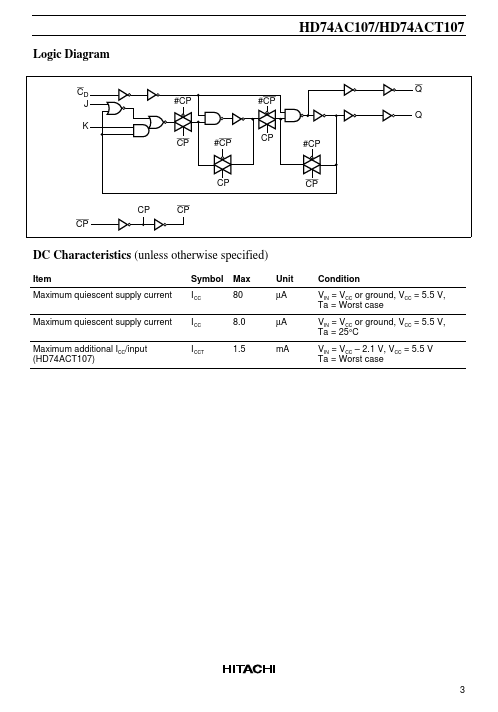
● Outputs Source/Sink 24 mA● HD74ACT107 has TTL-Compatible Inputs Pin Arrangement J1 1 Q1 2 Q1 3 K1 4 Q2 5 Q2 6 GND 7 (Top view) 14 VCC 13 CD1 12 CP1 11 K2 10 CD2 9 CP2 8 J2 HD74AC107/HD74ACT107 Logic Symbol 3 8 9 Q1 2 11 1 12 4 J1 CP1 K1 Q1 J2 CP2 K2 Q2 6 CD1 13 CD2 10 Q2 5 VCC = Pin14 GND = Pin7 Pin Names J1, J2, K1, K2 CP1, CP2 C D1, CD2 Q1, Q2, Q1, Q 2 Data Inputs Clock Pulse Inputs (Active Falling Edge) Direct Clear Inputs (Active Low) Outputs Truth Table Inputs @ tn J L L H H H L tn tn + 1 : : : : K L H L H High Voltage Level Low Voltage Level Bit time before clock pulse. Bit time after clock pulse. Outputs @ tn + 1 Q Qn L H Qn 2 HD74AC107/HD74ACT107 Logic Diagram CD J K CP #CP CP #CP Q #CP #CP Q CP CP CP CP CP DC Characteristics (unless otherwise specified) Item Maximum quiescent supply current Maximum quiescent supply current Maximum additional ICC/input (HD74ACT107) Symbol I CC I CC I CCT Max...