Hitachi HD74AC126
The HD74AC126/HD74ACT126 is an quad buffer and line driver designed to be employed as a memory address driver, clock driver and bus oriented transmitter/receiver which provides improved PC board density.| Part No. | HD74AC126 |
|---|---|
| Datasheet | HD74AC126 Download |
| Manufacturer |  Hitachi |
| Description | Quad Buffer/Line Driver with 3-State Output |
| Buy | Stock & Price |

DESCRIPTION
FEATURES
● 3-State Outputs Drive Bus Lines or Buffer Memory Address Registers● Outputs Source/Sink 24 mA
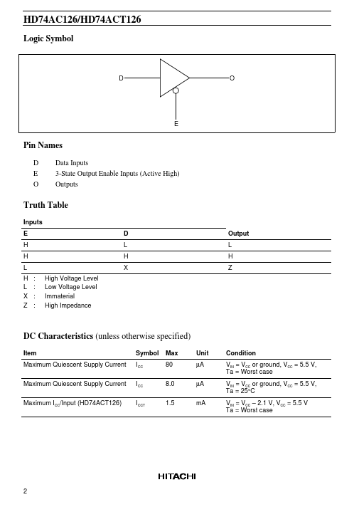
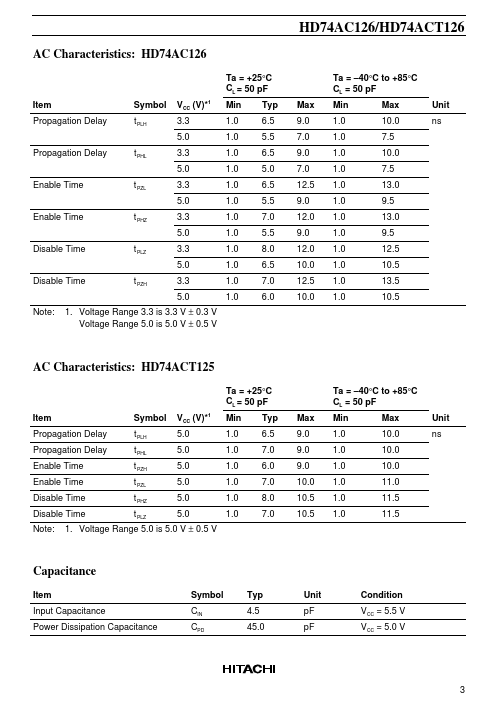
● HD74ACT126 has TTL-Compatible Inputs Pin Arrangement E 1 D 2 O 3 E 4 D 5 O 6 GND 7 (Top view) 14 VCC 13 E 12 D 11 O 10 E 9 D 8 O HD74AC126/HD74ACT126 Logic Symbol D O E Pin Names D E O Data Inputs 3-State Output Enable Inputs (Active High) Outputs Truth Table Inputs E H H L H L X Z : : : : High Voltage Level Low Voltage Level Immaterial High Impedance D L H X Output L H Z DC Characteristics (unless otherwise specified) Item Maximum Quiescent Supply Current Maximum Quiescent Supply Current Maximum ICC/Input (HD74ACT126) Symbol I CC I CC I CCT Max 80 8.0 1.5 Unit µA µA mA Condition VIN = VCC or ground, VCC = 5.5 V, Ta = Worst case VIN = VCC or ground, VCC = 5.5 V, Ta = 25°C VIN = VCC – 2.1 V, VCC = 5.5 V Ta = Worst case 2 HD74AC126/HD74ACT126 AC Characteristics: HD74AC126 Ta = +25°C CL = 50 pF Item Propagation Delay Symbol t PLH VCC (V)*1 3.3 5.0 Propagation Delay t PHL 3.3 5.0 Enable Time t PZL 3.3 5.0 Enable Time t PHZ 3.3 5.0 Disable Time t PLZ 3.3 5.0 Disable Time t PZH 3.3 5.0 Note: 1.