Hitachi HD74ALVC16836
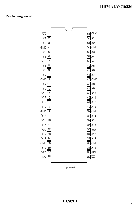
This 20-bit universal bus driver is designed for 2.3 V to 3.6 V VCC operation. The device operates in the transparent mode when the latch enable (LE) input is low.| Part No. | HD74ALVC16836 |
|---|---|
| Datasheet | HD74ALVC16836 Download |
| Manufacturer |  Hitachi |
| Description | 20-bit Universal Bus Driver with 3-state Outputs |
| Buy | Stock & Price |
DESCRIPTION
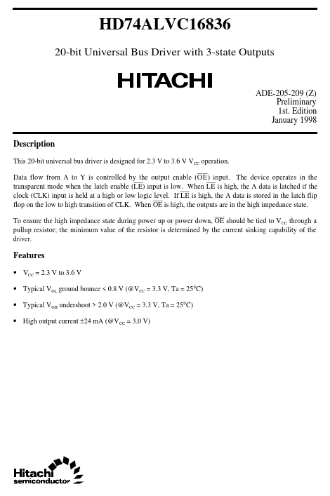
Data flow from A to Y is controlled by the output enable (OE ) input. When LE is high, the A data is latched if the clock (CLK) input is held at a high or low logic level. If LE is high, the A data is stored in the latch flip flop on the low to high transition of CLK. When OE is high, the outputs are in the high impedance state. To ensure the high impedance state during power up or power down, OE should be tied to V CC through a pullup resistor; the minimum value of the resistor is determined by the current sinking capability of the driver.FEATURES
● VCC = 2.3 V to 3.6 V● Typical VOL ground bounce < 0.8 V (@VCC = 3.3 V, Ta = 25°C)
● Typical VOH undershoot > 2.0 V (@VCC = 3.3 V, Ta = 25°C)
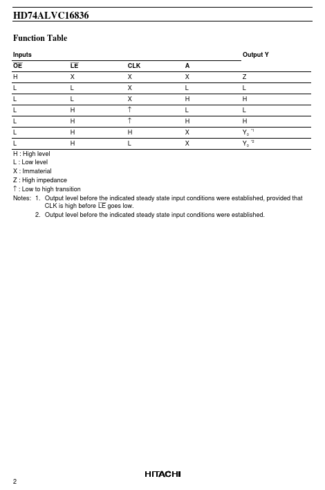
● High output current ±24 mA (@V CC = 3.0 V) HD74ALVC16836 Function Table Inputs OE H L L L L L L LE X L L H H H H CLK X X X ↑ ↑ H L A X L H L H X X Z L H L H Y0 Y0 *1 *2 Output Y H : High level L : Low level X : Immaterial Z : High impedance ↑ : Low to high transition Notes: 1. Output level before the indicated steady state input conditions were established, provided that CLK is high before LE goes low.