Hitachi HD74CDC857
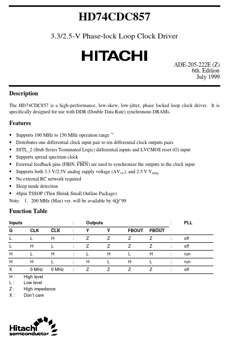
The HD74CDC857 is a high-performance, low-skew, low-jitter, phase locked loop clock driver. It is specifically designed for use with DDR (Double Data Rate) synchronous DRAMs.| Part No. | HD74CDC857 |
|---|---|
| Datasheet | HD74CDC857 Download |
| Manufacturer |  Hitachi |
| Description | 3.3/2.5-V Phase-lock Loop Clock Driver |
| Buy | Stock & Price |
DESCRIPTION
FEATURES
● Supports 100 MHz to 150 MHz operation range *1● Distributes one differential clock input pair to ten differential clock outputs pairs
● SSTL_2 (Stub Series Terminated Logic) differential inputs and LVCMOS reset (G) input
● Supports spread spectrum clock
● External feedback pins (FBIN, FBIN) are used to synchronize the outputs to the clock input
● Supports both 3.3 V/2.5V analog supply voltage (AV CC), and 2.5 V VDDQ
● No external RC network required
● Sleep mode detection
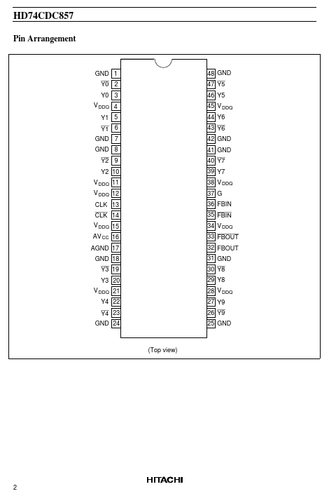
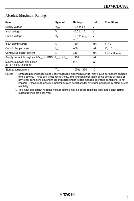
● 48pin TSSOP (Thin Shrink Small Outline Package) Note: 1. 200 MHz (Max) ver. will be available by 4Q/’99 Function Table Inputs G L L H H X H: L: Z: X: CLK L H L H 0 MHz CLK H L H L 0 MHz : : : : : : : Outputs Y Z Z L H Z Y Z Z H L Z FBOUT Z Z L H Z FBOUT Z Z H L Z : : : : : off off run run off : PLL High level Low level High impedance Don’t care HD74CDC857 Pin Arrangement GND 1 Y0 2 Y0 3 V DDQ 4 Y1 5 Y1 6 GND 7 GND 8 Y2 9 Y2 10 V DDQ 11 V DDQ 12 CLK 13 CLK 14 V DDQ 15 AV CC 16 AGND 17 GND 18 Y...