Hitachi HD74HC589
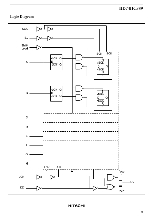
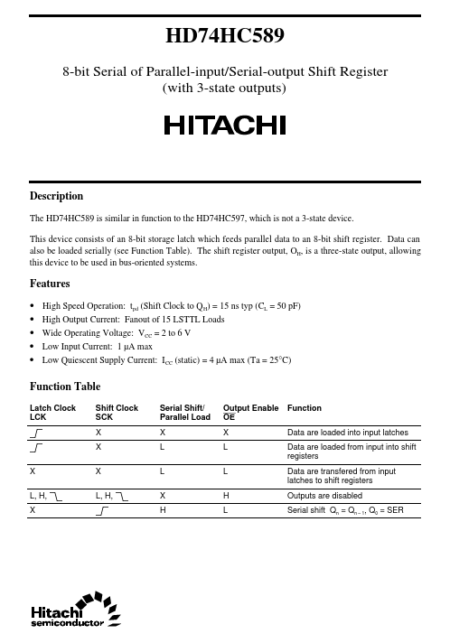
The HD74HC589 is similar in function to the HD74HC597, which is not a 3-state device. This device consists of an 8-bit storage latch which feeds parallel data to an 8-bit shift register. The shift register output, OH, is a three-state output, allowing this device to be used in bus-oriented systems.| Part No. | HD74HC589 |
|---|---|
| Datasheet | HD74HC589 Download |
| Manufacturer |  Hitachi |
| Description | 8-bit Serial of Parallel-input/Serial-output Shift Register |
| Buy | Stock & Price |
DESCRIPTION
Data can also be loaded serially (see Function Table).FEATURES
●●
●
●
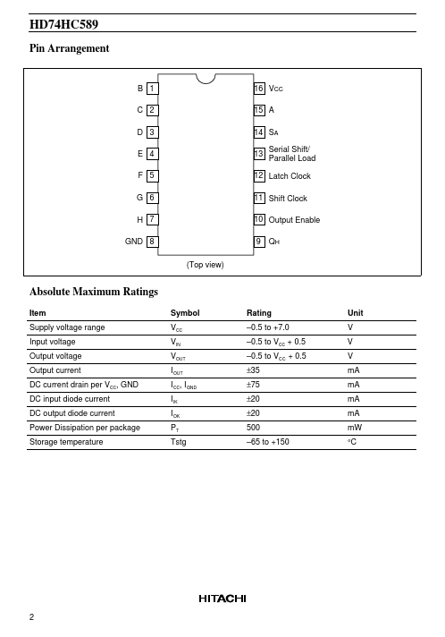
● High Speed Operation: tpd (Shift Clock to Q H) = 15 ns typ (CL = 50 pF) High Output Current: Fanout of 15 LSTTL Loads Wide Operating Voltage: VCC = 2 to 6 V Low Input Current: 1 µA max Low Quiescent Supply Current: ICC (static) = 4 µA max (Ta = 25°C) Function Table Latch Clock LCK Shift Clock SCK X X X L, H, X X L, H, Serial Shift/ Parallel Load X L L X H Output Enable OE X L L H L Function Data are loaded into input latches Data are loaded from input into shift registers Data are transfered from input latches to shift registers Outputs are disabled Serial shift Qn = Qn – 1, Q0 = SER HD74HC589 Pin Arrangement B 1 C 2 D 3 E 4 F 5 G 6 H 7 GND 8 (Top view) 16 VCC 15 A 14 SA 13 Serial Shift/ Parallel Load 12 Latch Clock 11 Shift Clock 10 Output Enable 9 QH
ABSOLUTE MAXIMUM RATINGS
Item Supply voltage range Input voltage Output voltage Output current DC current drain per VCC, GND DC input diode current DC output diode current Power Dissipation per package Storage temperature Symbol VCC VIN VOUT I OUT I CC, I GND I IK I OK PT Tstg Rating –0.5 to +7.0 –0.