Hitachi HD74HC75
This latch is ideally suited for use as temporary storage for binary information processing, input/output, and indicator units. The Q output will follow the data input as long as the enable remains high.| Part No. | HD74HC75 |
|---|---|
| Datasheet | HD74HC75 Download |
| Manufacturer |  Hitachi |
| Description | Quad. Bistable Latches |
| Buy | Stock & Price |
DESCRIPTION
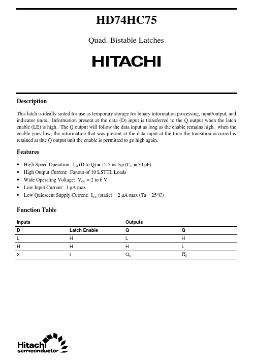
Information present at the data (D) input is transferred to the Q output when the latch enable (LE) is high. when the enable goes low, the information that was present at the data input at the time the transition occurred is retained at thte Q output unit the enable is permitted to go high again.FEATURES
●●
●
●
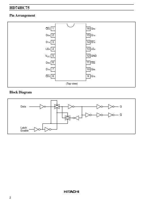
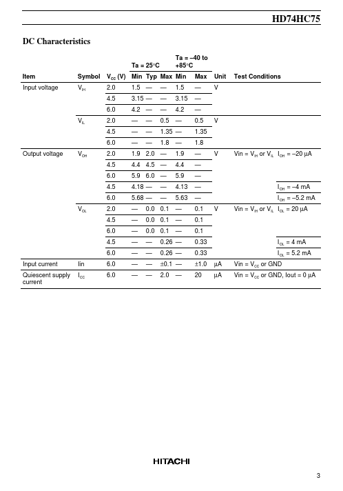
● High Speed Operation: tpd (D to Q) = 12.5 ns typ (C L = 50 pF) High Output Current: Fanout of 10 LSTTL Loads Wide Operating Voltage: VCC = 2 to 6 V Low Input Current: 1 µA max Low Quiescent Supply Current: ICC (static) = 2 µA max (Ta = 25°C) Function Table Inputs D L H X Latch Enable H H L Outputs Q L H Q0 Q H L Q0 HD74HC75 Pin Arrangement Q0a 1 D0a 2 D1a 3 LEb 4 VCC 5 D0b 6 D1b 7 Q1b 8 (Top view) 16 Q0a 15 Q1a 14 Q1a 13 LEa 12 GND 11 Q0b 10 Q0b 9 Q1b Block Diagram Data Q Q Latch Enable 2 HD74HC75 DC Characteristics Ta = 25°C Item Input voltage Symbol VIH Ta = –40 to +85°C Max — — — 0.5 1.35 1.8 — — — — — 0.1 0.1 0.1 0.33 0.33 ±1.0 20 µA µA I OL = 4 mA I OL = 5.2...