Hitachi HD74HCT08A
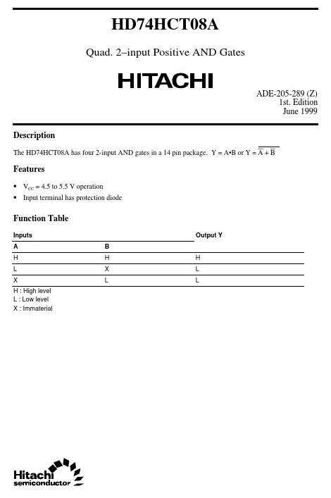
The HD74HCT08A has four 2-input AND gates in a 14 pin package.| Part No. | HD74HCT08A |
|---|---|
| Datasheet | HD74HCT08A Download |
| Manufacturer |  Hitachi |
| Description | Quad. 2-input Positive AND Gates |
| Buy | Stock & Price |
DESCRIPTION
Y = A●B or Y = A + BFEATURES
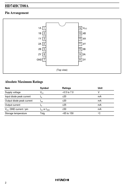
● VCC = 4.5 to 5.5 V operation● Input terminal has protection diode Function Table Inputs A H L X H : High level L : Low level X : Immaterial B H X L H L L Output Y HD74HCT08A Pin Arrangement 1A 1 1B 1Y 2 3 14 VCC 13 4B 12 4A 11 4Y 10 3B 9 3A 8 3Y 2A 4 2B 2Y 5 6 GND 7 (Top view)
ABSOLUTE MAXIMUM RATINGS
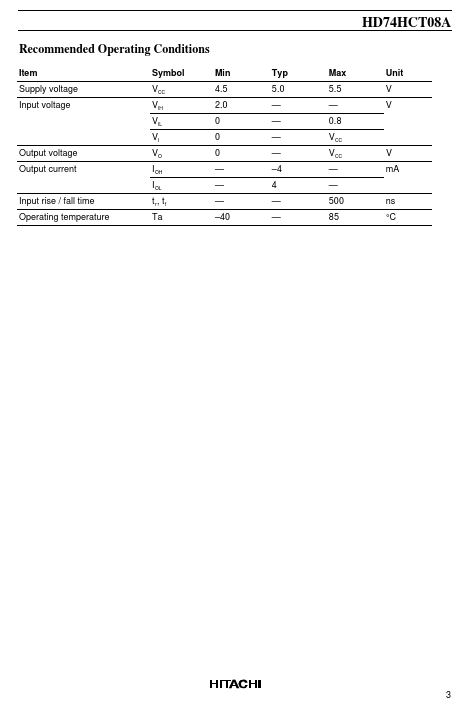
Item Supply voltage Input diode peak current Output diode peak current Output current VCC, GND current / pin Storage temperature Symbol VCC I IK I OK IO I CC or IGND Tstg Ratings –0.5 to 7.0 ±20 ±20 ±25 ±50 –65 to 150 Unit V mA mA mA mA °C 2 HD74HCT08A Recommended Operating Conditions Item Supply voltage Input voltage Symbol VCC VIH VIL VI Output voltage Output current VO I OH I OL Input rise / fall time Operating temperature t r, t f Ta Min 4.5 2.0 0 0 0 — — — –40 Typ 5.0 — — — — –4 4 — — Max 5.5 — 0.8 VCC VCC — — 500 85 ns °C V mA Unit V V 3 HD74HCT08A Logic Diagram (1/4 Circuit) A Y BELECTRICAL CHARACTERISTICS
Item Symbol VCC (V) Ta = 25°C Min Output voltage VOH 4.5 4.5 VOL 4.5 4.5 Input current Quiescent supply voltage II I CC 5.5 5.5 4.40 3.98 — — — — Typ — — — — ±0.1 — Max — — 0.10 0.