K1773 Overview
Key Specifications
Mount Type: Free Hanging
Pins: 73
Max Operating Temp: 175 °C
Min Operating Temp: -65 °C
Key Features
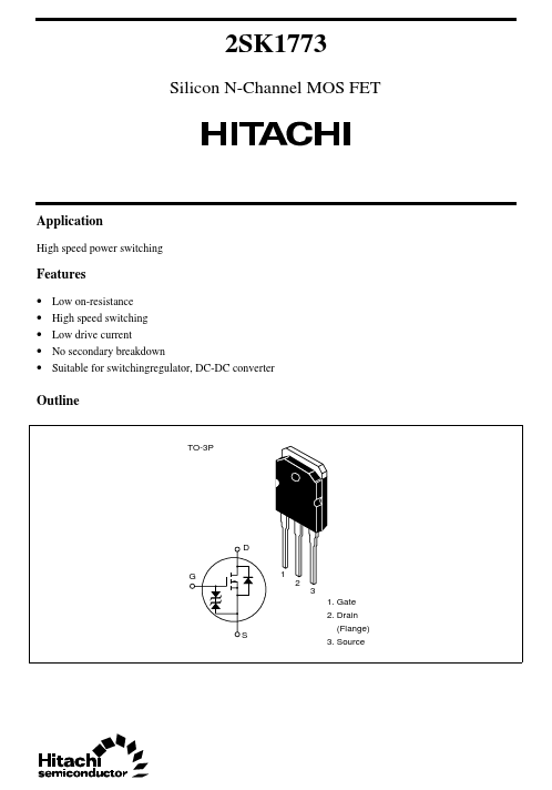
- Drain (Flange)
- Source S 2SK1773
| Part | K1773 |
|---|---|
| Description | Silicon N-Channel MOS FET |
| Manufacturer | Hitachi Semiconductor |
| Size | 48.07 KB |
Mount Type: Free Hanging
Pins: 73
Max Operating Temp: 175 °C
Min Operating Temp: -65 °C
| Seller | Inventory | Price Breaks | Buy |
|---|---|---|---|
| Newark | 13 | 1+ : 478.23 USD 5+ : 469.44 USD 10+ : 462.63 USD 25+ : 456.02 USD |
View Offer |
| Verical | 64 | 1+ : 400.8042 USD | View Offer |
| Part Number | Manufacturer | Description |
|---|---|---|
| K1771 | Toshiba | 2SK1771 |