K2728
Features
- Low on-resistance
- High speed switching
- Low drive current
- Avalanche ratings
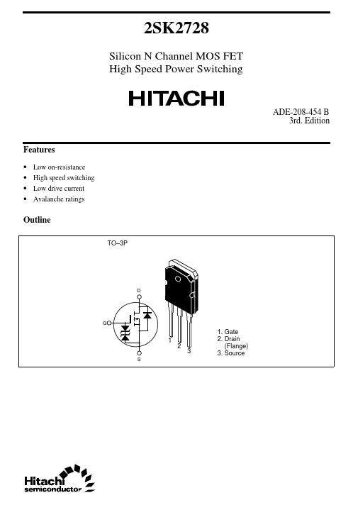
Outline
TO- 3P
ADE-208-454 B 3rd. Edition
1. Gate
1 2. Drain
2 3
(Flange) 3. Source
2SK2728
Absolute Maximum Ratings (Ta = 25°C)
Item
Symbol
Drain to source voltage Gate to source voltage Drain current Drain peak current Body to drain diode reverse drain current Avalanche current Avalanche energy Channel dissipation
VDSS VGSS ID I
- 1
D(pulse)
I DR I AP
- 3 EAR- 3 Pch- 2
Channel temperature
Tch
Storage temperature
Tstg
Notes: 1. PW ≤ 10µs, duty cycle ≤ 1 % 2. Value at Tc = 25°C 3. Value at Tch = 25°C, Rg ≥ 50Ω
Ratings 500 ±30 18 72 18 18 18 150 150
- 55 to +150
Unit V V A A A A m J W °C °C
Electrical Characteristics (Ta = 25°C)
Item
Symbol
Drain to source breakdown voltage
V(BR)DSS
Gate to source breakdown...