Hitachi LV74
The HD74LV74A has independent data, preset, clear, and clock inputs Q and Q outputs in a 14 pin package. The input data is transferred to the output at the rising edge of clock pulse CLK.| Part No. | LV74 |
|---|---|
| Datasheet | LV74 Download |
| Manufacturer |  Hitachi |
| Description | Dual D-type Flip Flops with Preset and Clear |
| Buy | Stock & Price |
DESCRIPTION
Low-voltage and high-speed operation is suitable for the battery-powered products (e.g., notebook computers), and the low-power consumption extends the battery life.FEATURES
●●
●
●
●
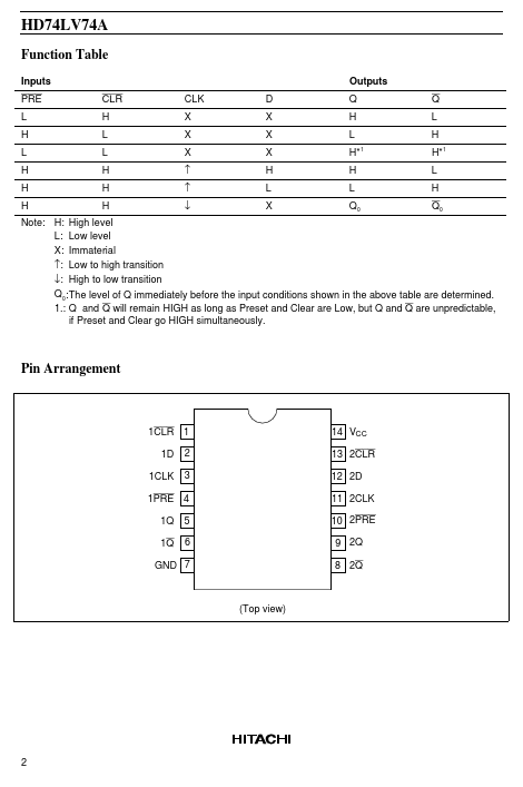
● VCC = 2.0 V to 5.5 V operation All inputs VIH (Max.) = 5.5 V (@VCC = 0 V to 5.5 V) All outputs VO (Max.) = 5.5 V (@VCC = 0 V) Typical VOL ground bounce < 0.8 V (@VCC = 3.3 V, Ta = 25°C) Typical VOH undershoot > 2.3 V (@VCC = 3.3 V, Ta = 25°C) Output current ±6 mA (@VCC = 3.0 V to 3.6 V), ±12 mA (@VCC = 4.5 V to 5.5 V) HD74LV74A Function Table Inputs PRE L H L H H H CLR H L L H H H CLK X X X ↑ ↑ ↓ D X X X H L X Outputs Q H L H* H L Q0 1 Q L H H*1 L H Q0 Note: H: High level L: Low level X: Immaterial ↑: Low to high transition ↓: High to low transition Q0:The level of Q immediately before the input conditions shown in the above table are determined. 1.: Q and Q will remain HIGH as long as Preset and Clear are Low, but Q and Q are unpredictable, if Preset and Clear go HIGH simultaneously. Pin A...