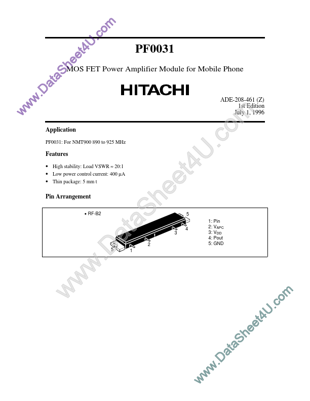
Datasheet4U Logo Datasheet4U.com

PF0031 - MOS FET Power Amplifier Module

Datasheet Summary

Features

  • High stability: Load VSWR ≈ 20:1.
  • Low power control current: 400 µA.
  • Thin package: 5 mm t Pin Arrangement.
  • RF-B2 w w . D w 5 t a 1 S a 2 e h 3 t e 5 4 U 4 . c m o 1: Pin 2: VAPC 3: VDD 4: Pout 5: GND w w w . D a S a t e e h U 4 t m o . c PF0031 Internal Diagram and External Circuit G GND Pin1 Pin Pin2 VAPC Pin3 VDD Pin4 Pout G GND Z1 C1 FB1 C3 FB2 C2 Z2 Pin VAPC VDD Pout C1 = C2 = 0.01 µF (Ceramic chip capacitor) C3 = 10 µF (Al.

📥 Download Datasheet

Datasheet preview – PF0031

Datasheet Details

Part number PF0031
Manufacturer Hitachi
File Size 81.58 KB
Description MOS FET Power Amplifier Module
Datasheet download datasheet PF0031 Datasheet
Additional preview pages of the PF0031 datasheet.
Other Datasheets by Hitachi

Full PDF Text Transcription

Click to expand full text
w w at .D w h FET Power Amplifier Module for Mobile Phone MOS S a ADE-208-461 (Z) 1st Edition July 1, 1996 ee U 4 t m o .c PF0031 Application PF0031: For NMT900 890 to 925 MHz Features • High stability: Load VSWR ≈ 20:1 • Low power control current: 400 µA • Thin package: 5 mm t Pin Arrangement • RF-B2 w w .D w 5 t a 1 S a 2 e h 3 t e 5 4 U 4 .c m o 1: Pin 2: VAPC 3: VDD 4: Pout 5: GND w w w .D a S a t e e h U 4 t m o .c PF0031 Internal Diagram and External Circuit G GND Pin1 Pin Pin2 VAPC Pin3 VDD Pin4 Pout G GND Z1 C1 FB1 C3 FB2 C2 Z2 Pin VAPC VDD Pout C1 = C2 = 0.
Published: |