2SD1419
2SD1419 is Silicon NPN Transistor manufactured by Hitachi Semiconductor.
Silicon NPN Epitaxial
Application
- Low frequency power amplifier
- plementary pair with 2SB1026
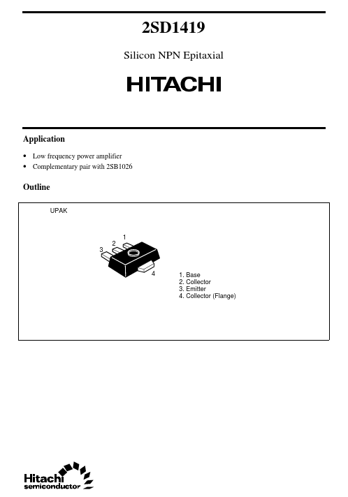
Outline
UPAK
1 3 2
1. Base 2. Collector 3. Emitter 4. Collector (Flange)
Absolute Maximum Ratings (Ta = 25°C)
Item Collector to base voltage Collector to emitter voltage Emitter to base voltage Collector current Collector peak current Collector power dissipation Junction temperature Storage temperature Symbol VCBO VCEO VEBO IC i C(peak)- PC
- Tj Tstg
2 1
Ratings 120 100 5 1 2 1 150
- 55 to +150
Unit V V V A A W °C °C
Notes: 1. PW ≤ 10 ms, Duty cycle ≤ 20% 2. Value on the alumina ceramic board (12.5 x 20 x 0.7 mm)
Electrical Characteristics (Ta = 25°C)
Item Collector to base breakdown voltage Symbol V(BR)CBO Min 120 100 5
- 1
Typ
- -
- -
- -
- - 140 12
Max
- -
- 10 200
- 1 1.5
- -
Unit V V V µA
Test conditions I C = 10 µA, IE = 0 I C = 1 m A, RBE = ∞ I E = 10 µA, IC = 0 VCB = 100 V, IE = 0 VCE = 5 V, IC = 150 m A- 2 VCE = 5 V, IC = 500 m A- 2 I C = 500 m A, IB = 50 m A- 2 VCE = 5 V, IC = 150 m A- 2 VCE = 5 V, IC = 150 m A- 2 VCB = 10 V, IE = 0, f = 1 MHz
Collector to emitter breakdown V(BR)CEO voltage Emitter to base breakdown voltage Collector cutoff current DC current transfer ratio V(BR)EBO I CBO h FE1- h FE2 Collector to emitter saturation voltage Base to emitter voltage Gain bandwidth product Collector output capacitance VCE(sat) VBE f T Cob
60 30
- -
- -
V V MHz p F
Notes: 1. The 2SD1419 is grouped by h FE1 as follows. 2. Pulse test Mark h FE1 DD 60 to 120 DE 100 to 200
See characteristic curves of 2SD1418.
Maximum Collector Dissipation Curve 1.2 Collector Power Dissipation PC (W) (on the alumina ceramic...