2SK1334
2SK1334 is Silicon N-Channel MOSFET manufactured by Hitachi Semiconductor.
Features
- -
- -
- Low on-resistance High speed switching Low drive current No secondary Breakdown Suitable for switching regulator and DC-DC converter
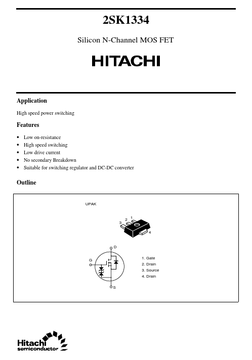
Outline
UPAK 2 1 4
D G 1. Gate 2. Drain 3. Source 4. Drain S
Absolute Maximum Ratings (Ta = 25°C)
Item Drain to source voltage Gate to source voltage Drain current Drain peak current Body to drain diode reverse drain current Channel dissipation Channel temperature Storage temperature Symbol VDSS VGSS ID I D(pulse)- I DR Pch- Tch Tstg
2 1
Ratings 200 ±20 1 2 1 1 150
- 55 to +150
Unit V V A A A W °C °C
Notes: 1. PW ≤ 10 µs, duty cycle ≤ 1% 2. When using the alumina ceramic board (12.5 × 20 × 0.7 mm)
Electrical Characteristics (Ta = 25°C)
Item Drain to source breakdown voltage Gate to source breakdown voltage Gate to source leak current Symbol Min V(BR)DSS V(BR)GSS I GSS 200 ±20
- - 2.0
- - Forward transfer admittance Input capacitance Output capacitance Reverse transfer capacitance Turn-on delay time Rise time Turn-off delay time Fall time Body to drain diode forward voltage Body to drain diode reverse recovery time |yfs| Ciss Coss Crss t d(on) tr t d(off) tf VDF t rr 0.4
- -
- -
- -
- -
- Typ
- -
- -
- 2.5 4.5 0.6 80 40 7 5 8 10 7 1.0 75 Max
- - ±10 50 4.0 3.8 7.0
- -
- -
- -
- -
- - Unit V V µA µA V Ω Ω S p F p F p F ns ns ns ns V ns I F = 1 A, VGS = 0 I F = 1 A, VGS = 0, di F/dt = 50 A/µs I D = 0.5 A, VGS = 10 V, RL = 60 Ω Test conditions I D = 10 m A, VGS = 0 I G = ±100 µA, VDS = 0 VGS = ±16 V, VDS = 0 VDS = 160 V, VGS = 0 I D = 1 m A, VDS = 10 V I D = 0.5 A, VGS = 10 V
- 1 I D = 2 A, VGS = 10 V
- 1 I D = 0.5 A, VDS = 10 V
- 1 VDS = 10 V, VGS = 0, f = 1 MHz
Zero gate voltage drain current I DSS Gate to source cutoff voltage Static drain to source on state resistance VGS(off) RDS(on)
Notes: 1. Pulse test 2. Marking for 2SK1334 is “BY”.
Power vs. Temperature Derating 1.2 Channel Dissipation Pch (W) Test Condition: When using alumina ceramic board(12.5×20×0.7mm) 0.8 Maximum Safe...